Integration of ALD tantalum nitride and alpha-phase tantalum for copper metallization application
What is AI technical title?
AI technical title is built by Patsnap AI team. It summarizes the technical point description of the patent document.
a technology of ald tantalum and alpha-phase tantalum, which is applied in the direction of coatings, special surfaces, chemical vapor deposition coatings, etc., can solve the problems of increasing the overall resistance, and reducing the reliability of the overall circui
Inactive Publication Date: 2003-07-03
APPLIED MATERIALS INC
View PDF99 Cites 199 Cited by
Summary
Abstract
Description
Claims
Application Information
AI Technical Summary
This helps you quickly interpret patents by identifying the three key elements:
Problems solved by technology
Method used
Benefits of technology
Problems solved by technology
However, copper diffuses more readily into surrounding materials and can alter the electronic device characteristics of the adjacent layers and, for example, form a conductive path between layers, thereby reducing the reliability of the overall circuit and possibly resulting in device failure.
Therefore, the additional amount of the barrier layer on the bottom of the feature not only increases the overall resistance of the feature, but also forms an obstruction between higher and lower metal interconnects of a multi-layered interconnect structure.
It is believed that the surface attraction used to physisorb, adsorb, absorb, or chemisorb a monolayer of reactants on a substrate surface are self-limiting in that only one monolayer may be deposited onto the substrate surface during a given pulse because the substrate surface has a finite number of sites available for the reactants.
While not wishing to be bound by theory, it is believed that a plasma treatment of a tantalum nitride film, for example, reduces the nitrogen content of one or more sublayers by sputtering off nitrogen, which in turn reduces resistivity.
It can be appreciated that a margin of error is present with this kind of measurement technique as well as any other measurement technique for determining a thickness of a deposited layer.
Method used
Image
Click on the blue label to locate the original text in one second.
Reading with bidirectional positioning of images and text.
Examples
Embodiment Construction
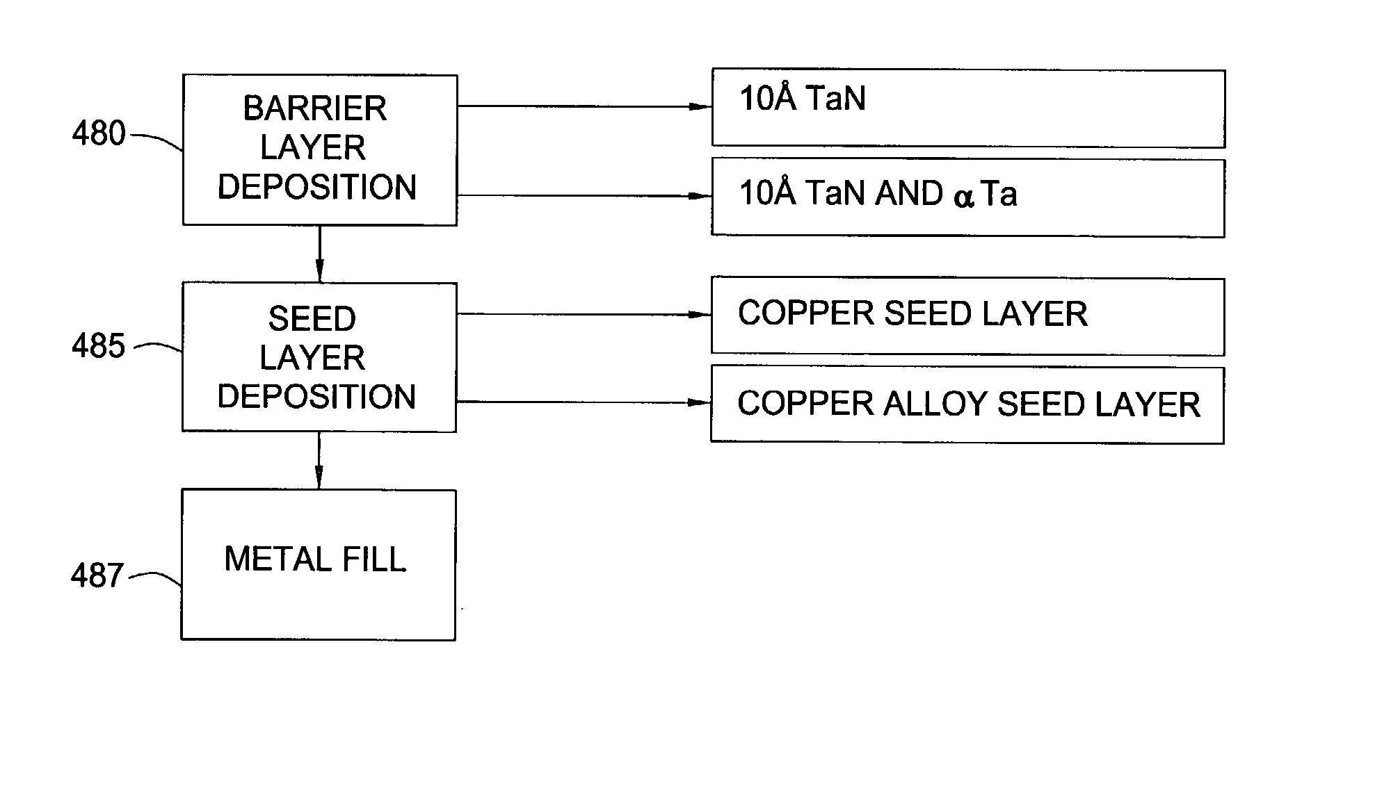
[0085] A TaN layer was deposited over a lower level copper layer using cyclical deposition to a thickness of about 20 .ANG.. A copper alloy seed layer was deposited over the TaN layer by physical vapor deposition to a thickness of about 100 .ANG.. The copper alloy seed layer contained aluminum in a concentration of about 2.0 atomic percent, and was deposited by PVD using a copper-aluminum target consisting of aluminum in a concentration of about 2.0 atomic percent. A bulk copper layer was then deposited using ECP to fill the feature. The substrate was then thermally annealed at a temperature of about 380.degree. C. for about 15 minutes in a nitrogen (N2) and hydrogen (H2) ambient.
[0086] The overall feature resistance was significantly reduced and the upper level copper layer surprisingly exhibited a grain growth similar to that of the lower level copper layer. The barrier performance of the TaN layer exhibited longer time to failure (TTF) compared with 50 .ANG. PVD Ta. Further, the ...
PUM
Property
Measurement
Unit
thickness
aaaaa
aaaaa
thickness
aaaaa
aaaaa
thickness
aaaaa
aaaaa
Abstract
A method for forming a metal interconnect on a substrate is provided. In one aspect, the method comprises depositing a refractory metal containing barrier layer having a thickness that exhibits a crystalline like structure and is sufficient to inhibit atomic migration on at least a portion of a metal layer by alternately introducing one or more pulses of a metal-containing compound and one or more pulses of a nitrogen-containing compound; depositing a seed layer on at least a portion of the barrier layer; and depositing a second metal layer on at least a portion of the seed layer.
Description
[0001] This application claims benefit of U.S. Provisional Patent Application Serial No. 60 / 346,086, filed on Oct. 26, 2001, and entitled "Method and Apparatus for ALD Deposition", which is incorporated by reference herein. This application also claims benefit of U.S. patent application, Ser. No. 09 / 965,370, filed on Sep. 26, 2001, and entitled "Integration of Barrier Layer and Seed Layer", which is incorporated by reference herein. This application also claims benefit of U.S. patent application Ser. No. 09 / 965,373, filed on Sep. 26, 2001, and entitled "Integration of Barrier Layer and Seed Layer", which is incorporated by reference herein. This application further claims benefit of U.S. patent application Ser. No. 09 / 965,369, filed on Sep. 26, 2001, and entitled "Integration of Barrier Layer and Seed Layer", which is incorporated by reference herein. This application further claims benefit of U.S. patent application Ser. No. 10 / 193,333, filed on Jul. 10, 2002, and entitled "Integra...
Claims
Application Information
Patent Timeline
Application Date:The date an application was filed.
Publication Date:The date a patent or application was officially published.
First Publication Date:The earliest publication date of a patent with the same application number.
Issue Date:Publication date of the patent grant document.
PCT Entry Date:The Entry date of PCT National Phase.
Estimated Expiry Date:The statutory expiry date of a patent right according to the Patent Law, and it is the longest term of protection that the patent right can achieve without the termination of the patent right due to other reasons(Term extension factor has been taken into account ).
Invalid Date:Actual expiry date is based on effective date or publication date of legal transaction data of invalid patent.
Patent Type & AuthorityApplications(United States)

