Method for achieving copper fill of high aspect ratio interconnect features

a technology of interconnect features and copper filling, which is applied in the direction of superimposed coating processes, semiconductor devices, coatings, etc., can solve the problems of void-free sub-micron formation, many traditional deposition processes have difficulty filling structures or features having sub-micron width, and many ongoing efforts are directed at the formation of void-free sub-microns

Inactive Publication Date: 2002-08-20
APPLIED MATERIALS INC
View PDF36 Cites 112 Cited by
  • Summary
  • Abstract
  • Description
  • Claims
  • Application Information

AI Technical Summary

Problems solved by technology

Many traditional deposition processes have difficulty filling structures or features having sub-micron width where the aspect ratio exceeds 4:1, and particularly where the ratio exceeds 10:1.
Thus, there is a great amount of ongoing effort being directed at the formation of void-free sub-micron features having high aspect ratios.
Despite the desirability of using copper for semiconductor device fabrication, choices of fabrication methods for depositing copper into very high aspect ratio features are limited because common chemical vapor deposition processes and physical vapor deposition processes have provided unsatisfactory results in forming void-free sub-micron features having high aspect ratios.
Furthermore, the vapor deposition processes can be costly.
However, a number of obstacles impair consistent electroplating of copper onto substrates having sub-micron high aspect ratio features.
Currently practiced physical vapor deposition methods encounters difficulty in forming a continuous, uniform seed layer within a sub-micron high aspect ratio feature.
The seed layer tends to become discontinuous on the sidewall surfaces and the bottom surface of the feature because of the difficulty in depositing into the narrow (i.e., nanometer-sized) aperture width of the feature.
The discontinuities in the seed layer prevent proper electroplating of metal onto the seed layer, resulting in defective devices on the processed substrate.
Second, it has been difficult to deposit into sub-micron high aspect ratio features without forming voids in the feature because the horizontal electroplated metal growth tends to close off the feature at the aperture opening before the feature has been completely filled, resulting in a void forming within the feature.
A void formation in the feature changes the material and operating characteristics of the interconnect feature, such as decreasing electromigration resistance, and typically causes improper operation and premature breakdown of the device.
However, the additional etching step to round-off corners of features increases the processing time for each substrate and reduces throughput of the system.
Furthermore, voids may still form within the features during the deposition process even with rounded corners at the feature opening.
Third, currently practiced electroplating methods have not provided consistent electroplating results between sequentially processed substrate in a single run.
Also, the material properties of the electroplated metal layer, such as grain size, orientation, reflectivity and resistance, are not sufficiently uniform across the deposited substrate surface of a single substrate when processed with typical electroplating systems.
However, rotation of the head assembly may not be necessary to achieve uniform electroplating deposition, particularly where the uniformity of electroplating deposition is achieved by adjusting the processing parameters, such as the electrolyte chemistry, electrolyte flow and other parameters.

Method used


Image

  • Method for achieving copper fill of high aspect ratio interconnect features
  • Method for achieving copper fill of high aspect ratio interconnect features
  • Method for achieving copper fill of high aspect ratio interconnect features

Examples


Embodiment Construction

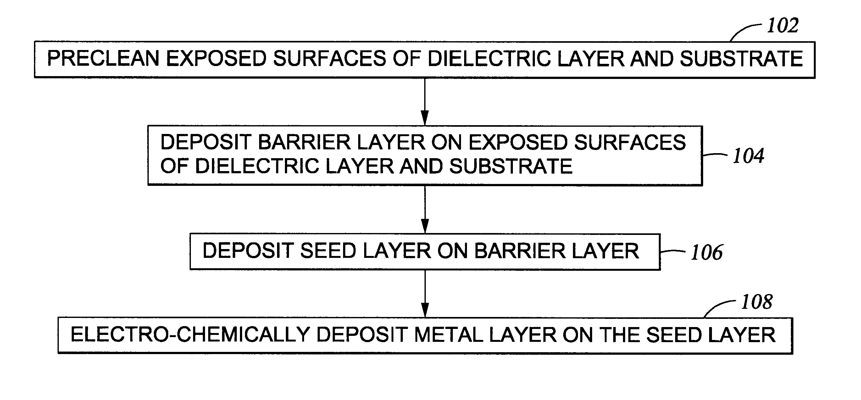
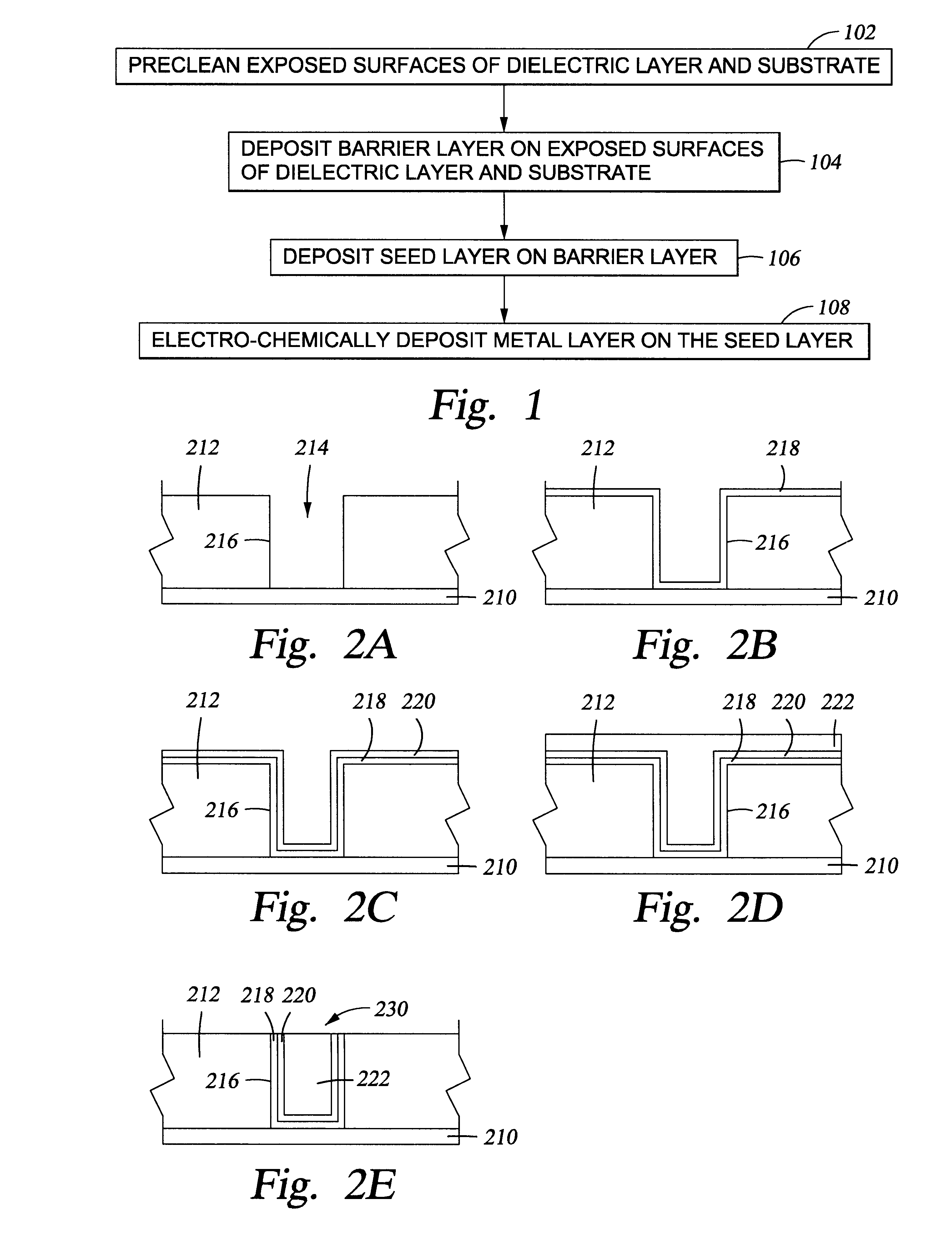
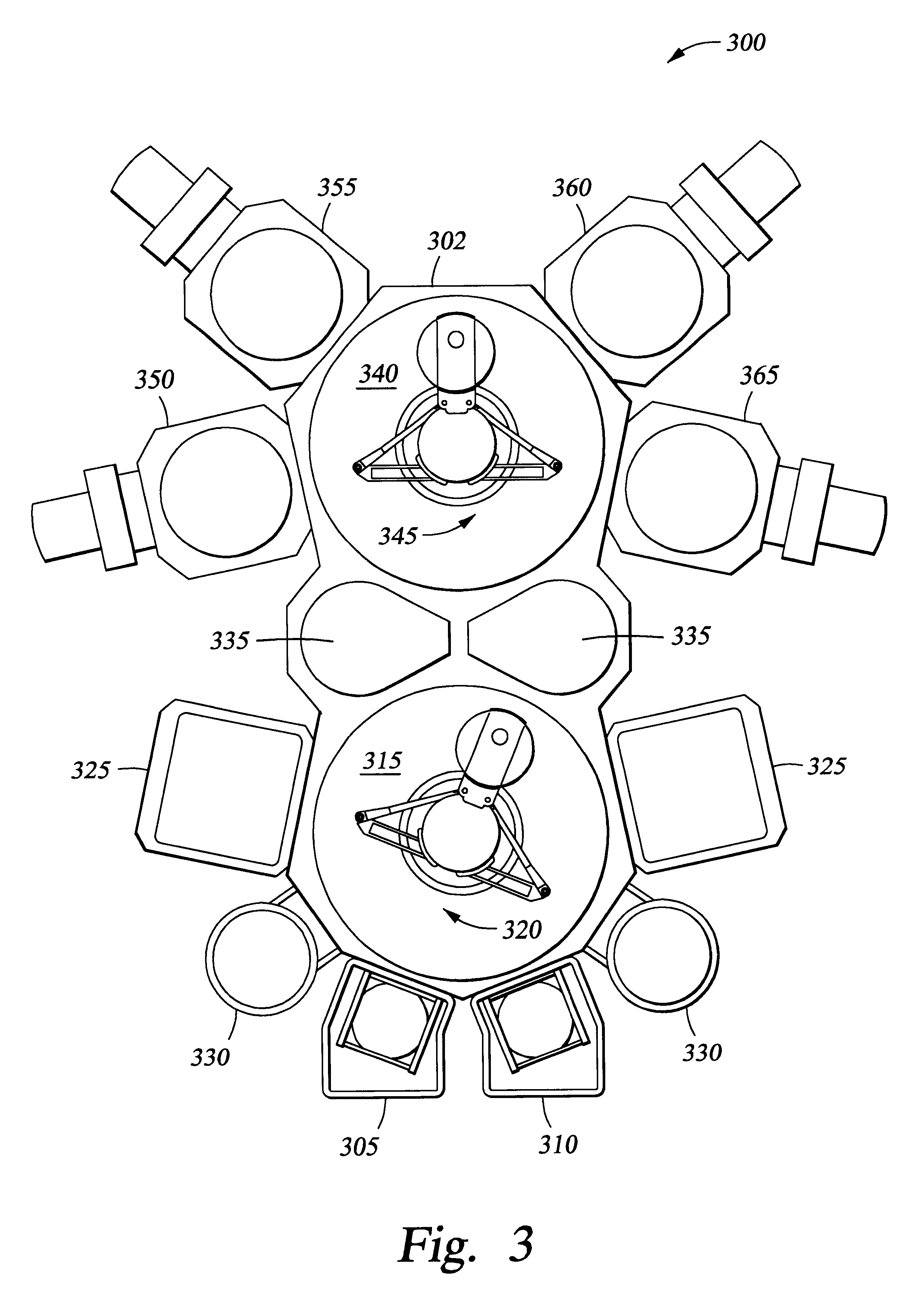
The present invention provides a method for filling sub-micron features on a substrate comprising reactive pre-cleaning the substrate; depositing a barrier layer on the substrate using high density plasma physical vapor deposition; depositing a seed layer over the barrier layer using high density plasma physical vapor deposition; and electro-chemically depositing a metal using a highly resistive electrolyte and applying a first current density during a first deposition period followed by a second current density during a second period. The steps of depositing the barrier layer and depositing the seed layer are performed in a high density plasma chamber, and the electroplating process is performed in an electroplating cell.

To begin the pre-clean process, a substrate having sub-micron, high aspect ratio interconnect features is transferred into a pre-clean chamber. A pre-clean gas mixture comprising about 5% hydrogen and about 95% helium is introduced into the chamber, and the chamber...


PUM

PropertyMeasurementUnit
current densityaaaaaaaaaa
molar concentrationaaaaaaaaaa

Abstract

One aspect of the invention provides a consistent metal electroplating technique to form void-less metal interconnects in sub-micron high aspect ratio features on semiconductor substrates. One embodiment of the invention provides a method for filling sub-micron features on a substrate, comprising reactive precleaning the substrate, depositing a barrier layer on the substrate using high density plasma physical vapor deposition; depositing a seed layer over the barrier layer using high density plasma physical vapor deposition; and electro-chemically depositing a metal using a highly resistive electrolyte and applying a first current density during a first deposition period followed by a second current density during a second period.

Description

1. Field of the InventionThe invention generally relates to semiconductor processing. More particularly, the invention relates to metallization of sub-micron interconnect features on a substrate.2. Background of the Related ArtCopper has become a choice metal for filling sub-micron, high aspect ratio interconnect features on substrates as circuit densities increase for the next generation of ultra large scale integration because copper and copper alloys have lower resistivity than aluminum and significantly higher electromigration resistance as compared to aluminum. These characteristics are important for supporting the higher current densities experienced at high levels of integration and increased device speed.The aspect ratios for the features, i.e., the ratio for the feature height to the feature width, increases with the higher level of integration. Many traditional deposition processes have difficulty filling structures or features having sub-micron width where the aspect rati...

Claims


Application Information

Patent Timeline
Patent Type & Authority Patents(United States)
IPC IPC(8): H01L21/02H01L21/768H01L21/288H01L21/70
CPCH01L21/2885H01L21/76877
Inventor CARL, DANIEL A.CHIN, BARRYCHEN, LIANGCHEUNG, ROBINDING, PEIJUNDORDI, YEZDIHASHIM, IMRANHEY, PETERSINHA, ASHOK K.
Owner APPLIED MATERIALS INC
Why Eureka
Try Eureka