Static random access memory device and method for manufacturing the same

a random access memory and random access technology, applied in semiconductor devices, digital storage, instruments, etc., can solve the problems of increasing manufacturing costs, complicated process, and less integration density

Inactive Publication Date: 2002-07-09
SAMSUNG ELECTRONICS CO LTD
View PDF1 Cites 126 Cited by
  • Summary
  • Abstract
  • Description
  • Claims
  • Application Information

AI Technical Summary

Problems solved by technology

Thus, it has high cell area, resulting in the disadvantage of less integration density, compared to the other two types of cells, which require only four transistors.
Merging the SRAM cell of FIG. 2 with a logic device requires additional processes based on a general CMOS standard logic manufacturing process, th...

Method used


Image

  • Static random access memory device and method for manufacturing the same
  • Static random access memory device and method for manufacturing the same
  • Static random access memory device and method for manufacturing the same

Examples


Embodiment Construction

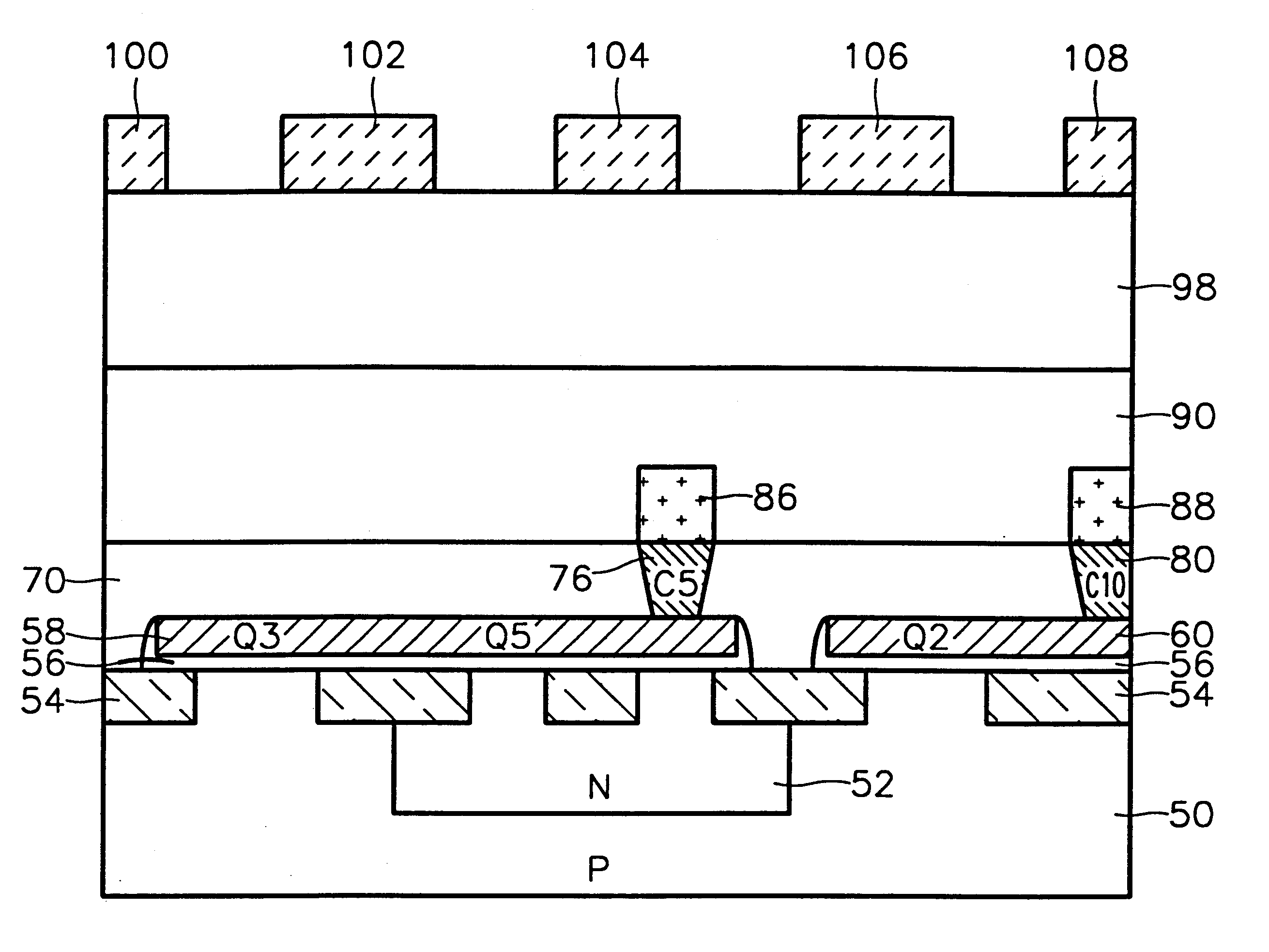
The present invention now will be described more fully with reference to the accompanying drawings. In the drawings, the thickness of layers and regions are exaggerated for clarity.

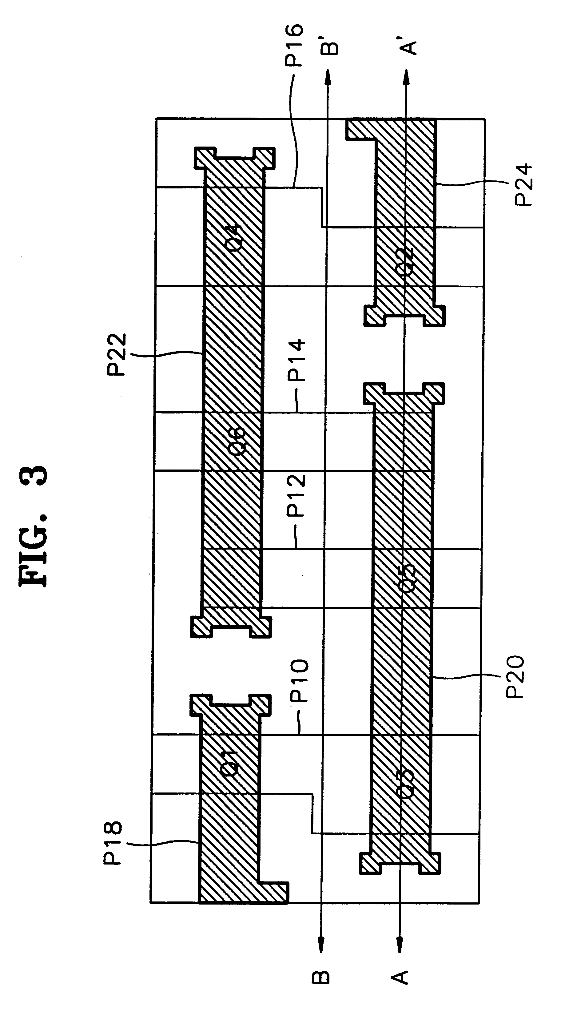
FIGS. 3 through 9 are layouts of exemplary mask patterns for use in manufacturing a static random access memory (SRAM) device by a standard CMOS logic manufacturing process without need for additional masks or processes, in accordance with an embodiment of the present invention. In particular, referring to FIG. 3, the layout of mask patterns for use in forming active regions and gates are shown. Reference symbol P10 represents the mask pattern for forming a first active region, reference symbol P12 represents the mask pattern for forming a third active region, reference symbol P14 represents the mask pattern for forming a fourth active region, reference symbols P16 represents the mask pattern for forming a second active region, reference symbol P18 represents the mask pattern for forming the gate of the f...


PUM


Abstract

A static random access memory (SRAM) device and a method for manufacturing the same are disclosed. In the SRAM device including a flip-flop circuit including two access transistors and a pair of inverters, connection lines for connecting the inputs and outputs of the inverters, and a word line, power supply lines and bit lines are formed of a metal interconnection. The resistance of interconnection can be reduced and the SRAM device manufacturing process can be performed along with CMOS standard logic manufacturing process.

Description

1. Field of the InventionThe present invention relates to a semiconductor device and a method for manufacturing the same, and more particularly, to a static random access memory device (SRAM) which can be manufactured by a CMOS standard logic manufacturing process and a method for manufacturing the same.2. Description of the Related ArtStatic random access memories (SRAMs) are easy to use and operate faster compared to dynamic random access memories (DRAM). For these reasons, the SRAMs have been used typically as a cache memory or a system memory in terminals. Recently, a development tendency of semiconductor devices towards high performance and composite functionality has raised use of SRAM embedded logic products, in which SRAMs and logic products are merged in one chip.Referring to FIG. 1, an equivalent circuit diagram of a unit memory cell of a general SRAM device is shown. As shown in FIG. 1, the SRAM cell is composed of two access transistors Q1 and Q2 and a flip-flop circuit ...

Claims


Application Information

Patent Timeline
IPC IPC(8): H01L29/72H01L21/70H01L27/11H01L29/66H01L21/8244
CPCH01L27/11H01L27/1104H10B10/00H10B10/12
Inventor OH, CHANG-BONG
Owner SAMSUNG ELECTRONICS CO LTD
Why Eureka
Try Eureka