

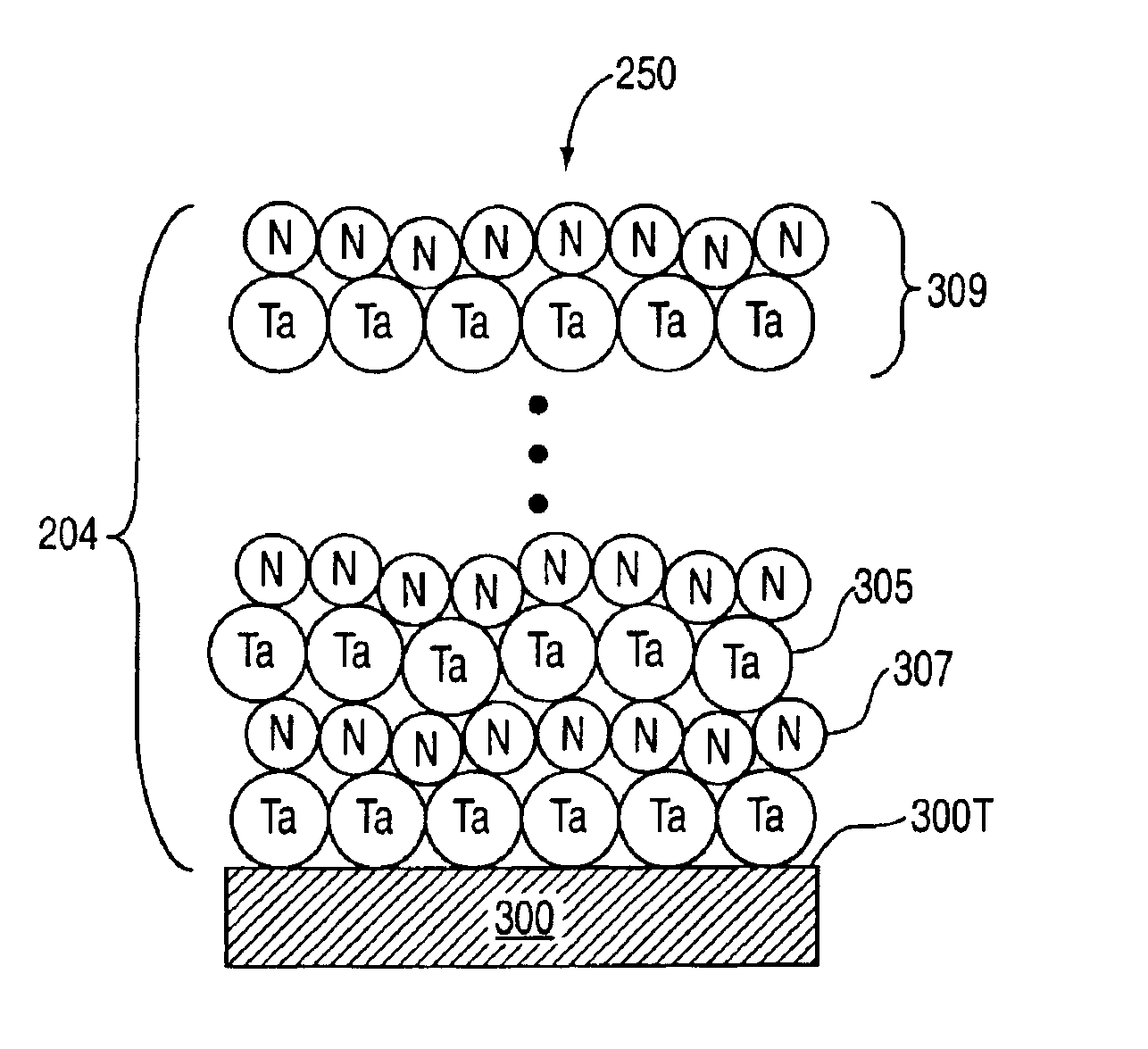
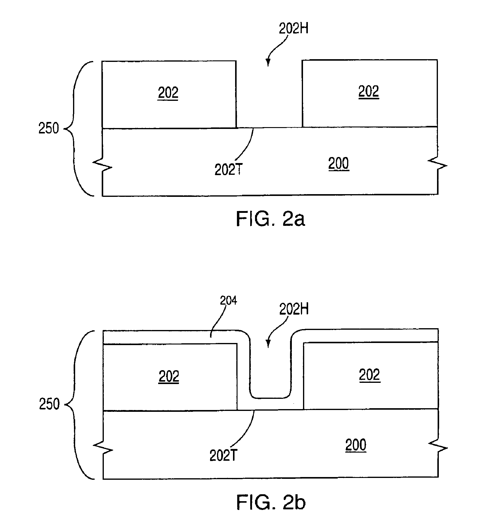
Formation of a tantalum-nitride layer
a technology of tantalum nitride and barrier layer, which is applied in the direction of coating, metallic material coating process, chemical vapor deposition coating, etc., can solve the problems of high chlorine content, reliability problems, and degradation of integrated circuits
- Summary
- Abstract
- Description
- Claims
- Application Information
AI Technical Summary
Benefits of technology
Problems solved by technology
Method used
Image

Examples
Embodiment Construction
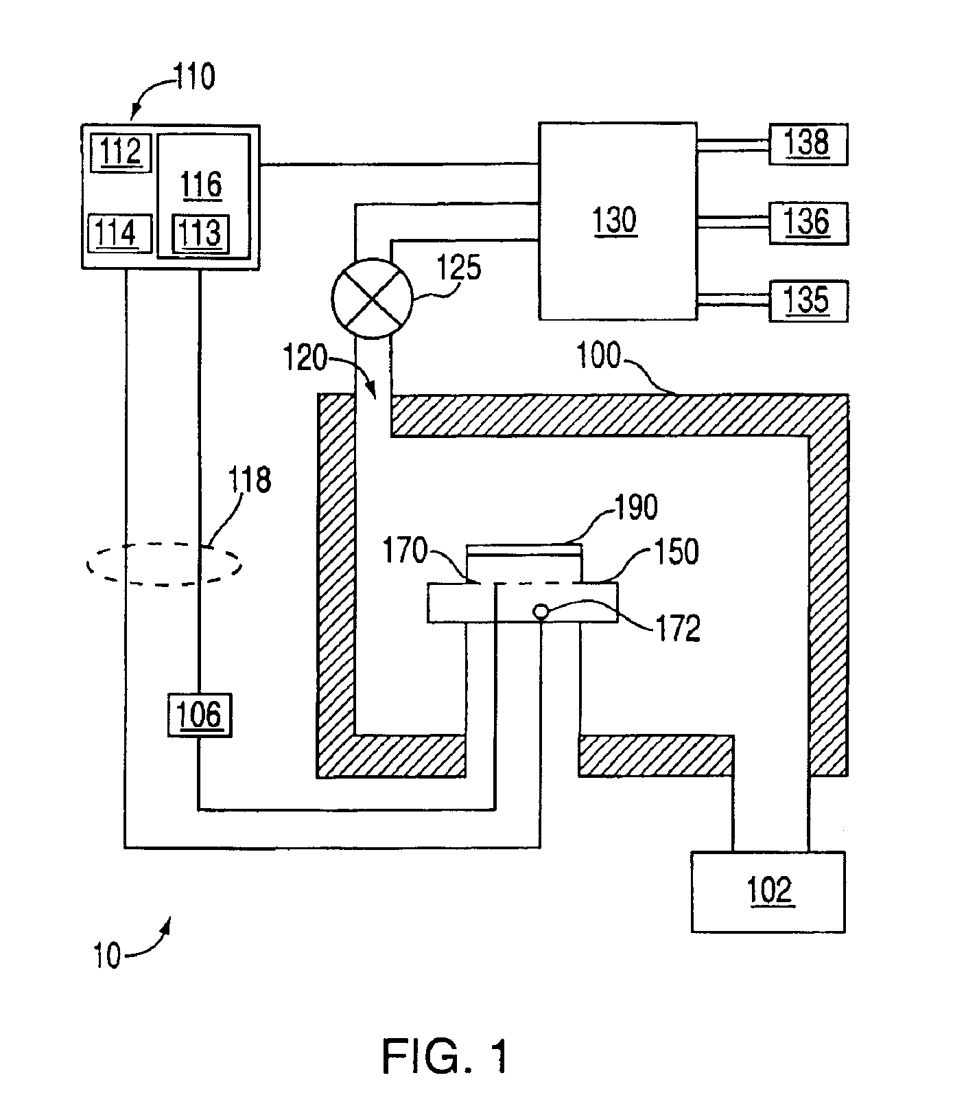
[0018]FIG. 1 depicts a schematic illustration of a wafer processing system 10 that can be used to form one or more tantalum-nitride barrier layers in accordance with aspects of the present invention described herein. System 10 comprises process chamber 100, gas panel 130, control unit 110, along with other hardware components such as power supply 106 and vacuum pump 102. For purposes of clarity, salient features of process chamber 100 are briefly described below.
Process Chamber
[0019]Process chamber 100 generally houses a support pedestal 150, which is used to support a substrate such as a semiconductor wafer 190 within process chamber 100. Depending on process requirements, semiconductor wafer 190 can be heated to some desired temperature or within some desired temperature range prior to layer formation using heater 170.
[0020]In chamber 100, wafer support pedestal 150 is heated by an embedded heating element 170. For example, pedestal 150 may be resistively heated by applying an ele...
PUM
| Property | Measurement | Unit |
|---|---|---|
| temperature | aaaaa | aaaaa |
| pressure | aaaaa | aaaaa |
| temperature | aaaaa | aaaaa |
Abstract
Description
Claims
Application Information