

Light emitting device
Inactive Publication Date: 2003-08-07
SEMICON ENERGY LAB CO LTD
View PDF0 Cites 87 Cited by
- Summary
- Abstract
- Description
- Claims
- Application Information
AI Technical Summary
Problems solved by technology
However, there are basically only a small number of organic materials capable of changing in accordance with the phosphorescent deactivation process at room temperature.
Thereafter, while holes are injected into the electron transporting layer because of a small ionization potential difference between the hole transporting layer and the electron transporting layer, electrons are blocked by the hole transporting layer to be confined in the electron transporting layer without being injected into the hole transporting layer because the electrical affinity of the hole transporting layer is low and because the difference between the electrical affinities of the hole transporting layer and the electron transporting layer is excessively large.
Although triplet light emitting devices have light emission efficiency much higher than that of singlet light emitting devices, they are incomparably shorter in life than singlet light emitting materials and lack stability.
Therefore triplet light emitting devices simply have the drawback of requiring much time and labor for fabrication.
In Reference 8, low stability of BCP used as a hole blocking material is mentioned as a cause of the limitation of life.
While efficient carrier recombination can be achieved by the carrier confinement effect of the hole blocking layer, the life of the device is limited because the hole blocking material ordinarily used is considerably low in stability.
Also, CBP used as a host material is also low in stability and is also considered to be a cause of the limitation of the life.
BCP is, of course, lower in stability than any other material, so that the stability of the device is low, while the efficiency is high.
In this device, however, CBP is used as a host material, so that the stability is low, while the light emission efficiency is high.
As
Method used
View moreImage
Smart ImageViewing Examples

Examples
 PUM
 Abstract
A triplet light emitting device which has high efficiency and improved stability and which can be fabricated by a simpler process is provided by simplifying the device structure and avoiding use of an unstable material. In a multilayer device structure using no hole blocking layer conventionally used in a triplet light emitting device, that is, a device structure in which on a substrate, there are formed an anode, a hole transporting layer constituted by a hole transporting material, an electron transporting and light emitting layer constituted by an electron transporting material and a dopant capable of triplet light emission, and a cathode, which are laminated in the stated order, the combination of the hole transporting material and the electron transporting material and the combination of the electron transporting material and the dopant material are optimized.
Description
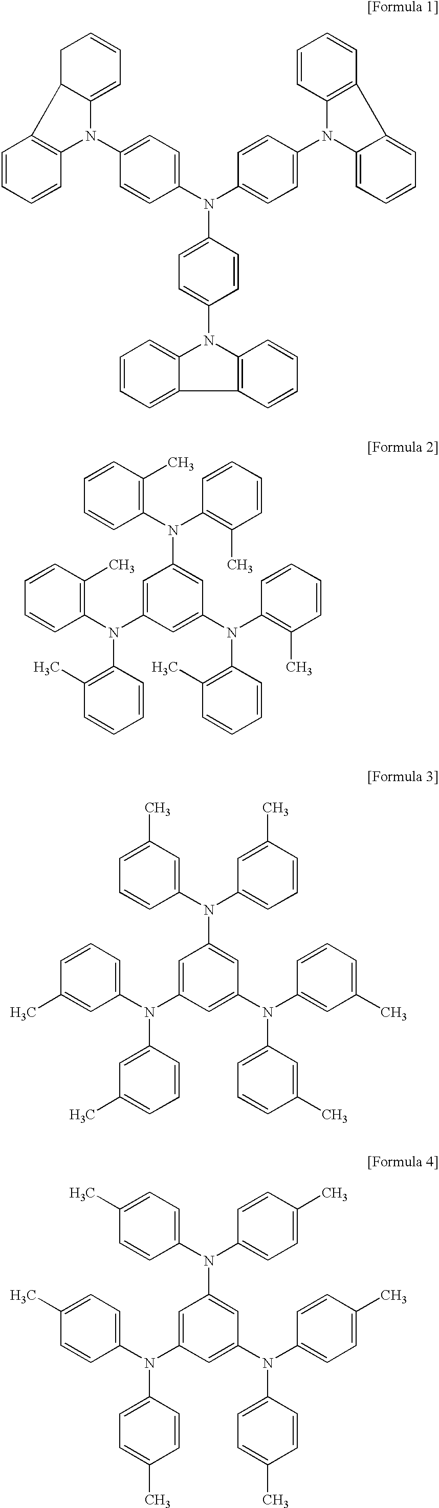
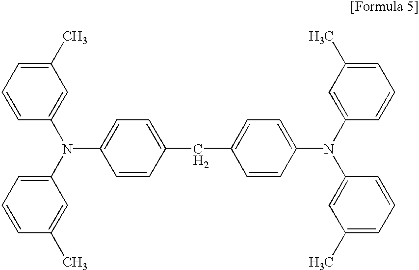
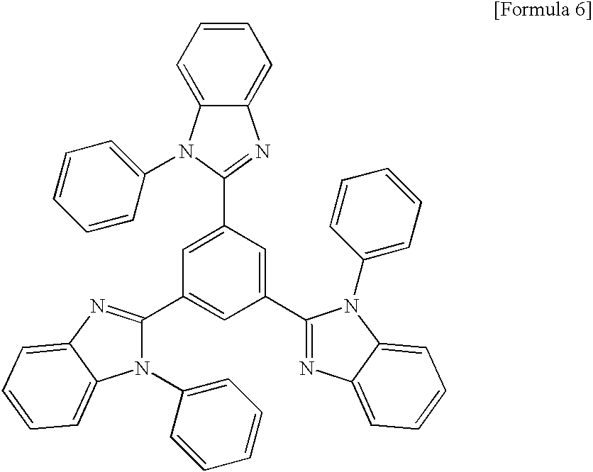
[0001] 1. Field of the Invention[0002] The present invention relates to an organic light emitting device constituted by an anode, an organic compound film capable of emitting light under the action of an electric field, and a cathode. In particular, the present invention relates to an organic light emitting device using a light emitting material which emits light in a triplet exited state.[0003] 2. Description of the Related Art[0004] An organic light emitting device is a device designed by utilizing a phenomenon in which electrons and holes are caused to flow into an organic compound film through two electrodes by application of a voltage to cause emission of light from molecules in an excited state (excited molecules) formed by recombination of the electrons and holes.[0005] Emission of light from an organic compound is a conversion into light of energy released when excited molecules are formed and then deactivated into the ground state. Deactivation processes causing such emissi...
Claims
Login to View More Application Information
Patent Timeline
 IPC IPC(8): H01L51/00H01L51/30H01L51/50
CPCH01L51/0059H01L51/508H01L51/0071H01L51/0072H01L51/0077H01L51/0079H01L51/008H01L51/0081H01L51/0085H01L51/0094H01L51/5016H01L51/5048H01L2251/552Y10S428/917H01L51/5056H01L51/0062H10K85/649H10K85/631H10K85/30H10K85/321H10K85/322H10K85/6572H10K85/657H10K85/324H10K85/342H10K85/40H10K50/11H10K2101/10H10K50/14H10K2101/30H10K50/15H10K50/166H10K85/636H10K50/16H10K50/81H10K50/828
InventorYAMAZAKI, HIROKOTOKUDA, ATSUSHITSUTSUI, TETSUO
OwnerSEMICON ENERGY LAB CO LTD