Light Emitting Element and Light Emitting Device

a light-emitting element and light-emitting device technology, applied in the field of organome, can solve the problems of wasting at least 75% of injected carriers, not easily generating noise, and -emitting element using a triplet luminescent material has a problem with the lifetime, so as to achieve high luminous efficiency, long lifetime, and large energy gap

Inactive Publication Date: 2007-10-18
SEMICON ENERGY LAB CO LTD
View PDF28 Cites 50 Cited by
  • Summary
  • Abstract
  • Description
  • Claims
  • Application Information

AI Technical Summary

Benefits of technology

[0055] According to the present invention, an organometallic complex that is capable of emitting phosphorescence can be obtained. In addition, a light-emitting element that has a light-emitting layer including the organometallic complex and a compound that has a larger energy gap than the organometallic complex can be driven for a long time, is high in luminous efficiency, and has a long lifetime. By using the organometallic complex according to the present invention as a luminescent material, a light-emitting element that is capable of providing red or reddish luminescence that is excellent in chromaticity can b

Problems solved by technology

Further, since such a light-emitting element is a carrier-injection light-emitting element, driving by a direct voltage is possible, and noise is not easily generated.
In other words, in the case of a light-emitting element using a fluorescent material, at least 75% of injected carriers are wasted useless

Method used


Image

  • Light Emitting Element and Light Emitting Device
  • Light Emitting Element and Light Emitting Device
  • Light Emitting Element and Light Emitting Device

Examples


embodiment mode 1

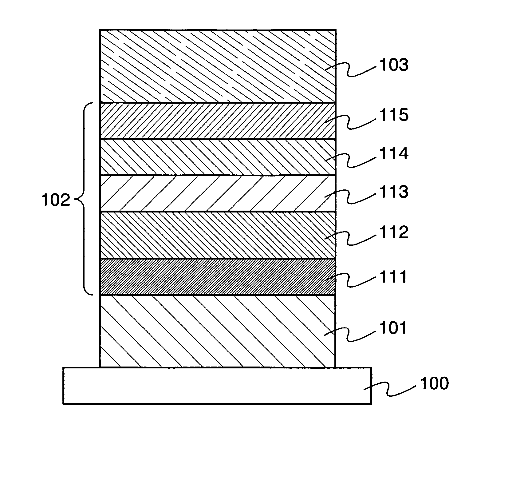
[0124] In Embodiment mode 1, a light-emitting element according to the present invention will be described with reference to FIG. 1.

[0125] As shown in FIG. 1, the light-emitting element according to the present invention has a structure in which a first electrode 101 is formed on a substrate 100, a layer 102 including a luminescent material is formed on the first electrode 101, and a second electrode 103 is formed thereon. As a material to be used for the substrate 100 here, a material that is used for a conventional light-emitting element may be used. For example, glass, quartz, transparent plastic, and a flexible substrate can be used. In addition, the first electrode 101 and the second electrode 103 in Embodiment mode 1 function as an anode and a cathode, respectively.

[0126] Namely, the first electrode 101 is formed by using an anode material. As the anode material that can be used here, it is preferable to use a metal, an alloy, an electrically conductive compound, or a mixtur...

embodiment mode 2

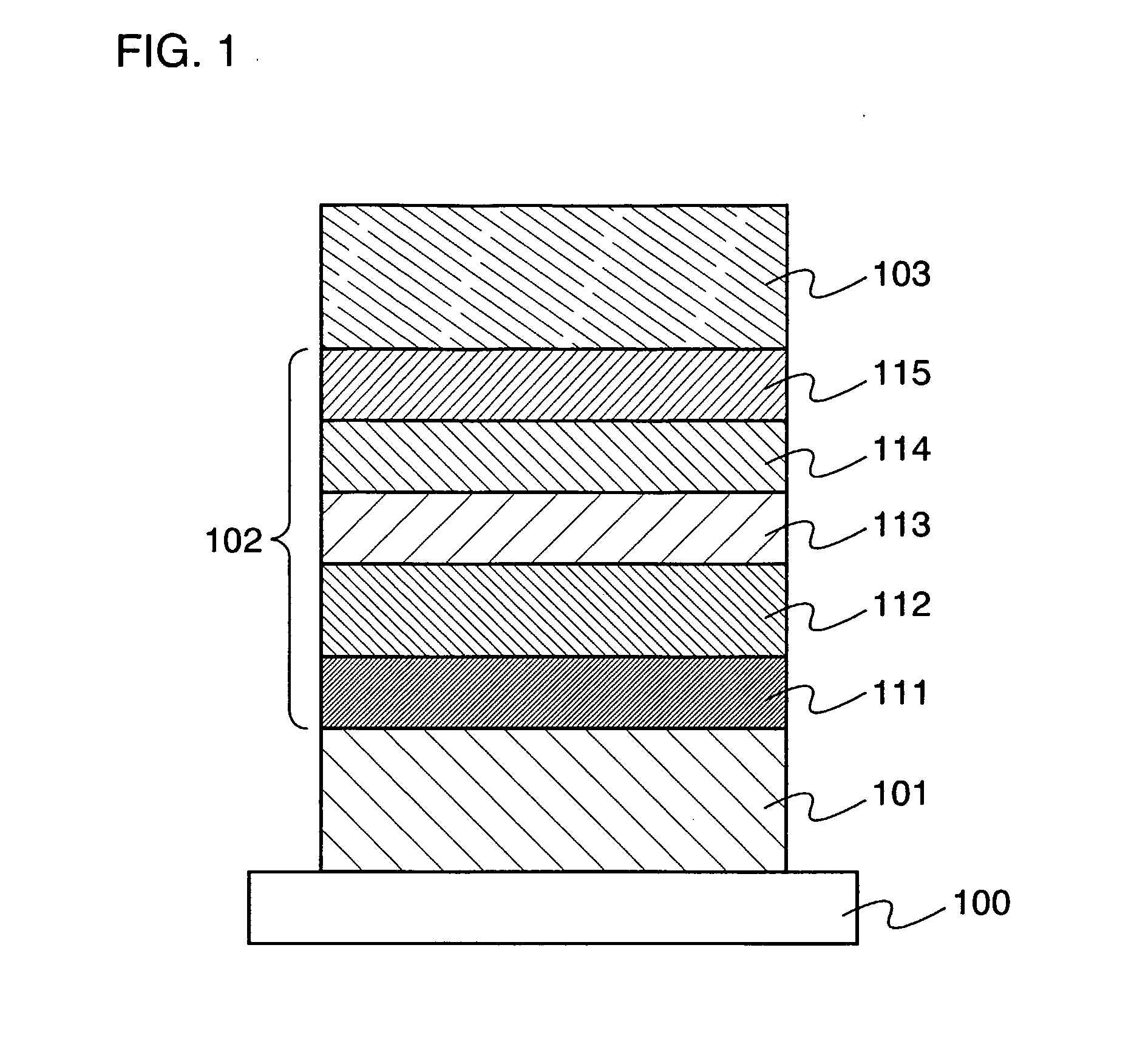
[0143] A light-emitting element according to the present invention will be described with reference to FIG. 2.

[0144] The light-emitting element shown in FIG. 2 has a first electrode 201 on a substrate 200 to serve as a cathode, a layer 202 including a luminescent material on the first electrode, and a second electrode 203 on the layer 202 including the luminescent material to serve as an anode. As shown in FIG. 2, the layer 202 including the luminescent material is formed by stacking an electron transporting layer 211, a hole blocking layer 212, a light-emitting layer 213, a hole transporting layer 214, and a hole injecting layer 215 in order, where the electron transporting layer 211 and the hole transporting layer 214 are provided respectively on the first electrode 201 side and on the second electrode 203 side with the light-emitting layer 213 as a center.

[0145] The electron transporting layer 211, the hole blocking layer 212, the light-emitting layer 213, the hole transporting...

embodiment mode 3

[0147] In Embodiment mode 3, a light-emitting element using an organometallic complex according to the present invention is manufactured over a substrate 300 composed of glass, quartz, a metal, a bulk semiconductor, transparent plastics, a flexible substrate, or the like. By manufacturing a plurality of light-emitting elements using the organometallic complex according to the present invention over a substrate, a passive matrix light-emitting device can be manufactured. In addition, other than a substrate composed of glass, quartz, transparent plastics, a flexible substrate, or the like, for example, a light-emitting element in contact with a thin film transistor (TFT) array may be manufactured as shown in FIG. 3 where a light-emitting element 313 is manufactured together with TFTs 311 and 312.

[0148] For the light-emitting element 313, a first electrode 314, a layer 315 including a luminescent material, and a second electrode 316 can be manufactured. Further, a wiring 317 is manufa...


PUM

PropertyMeasurementUnit
Energy gapaaaaaaaaaa

Abstract

It is an object of the present invention to obtain an organometallic complex that is capable of converting an excited triplet state into luminescence, a light-emitting element that can be driven for a long time, is high in luminous efficiency, and has a favorable long lifetime, and a light-emitting device using the light-emitting element. The present invention provides a light-emitting element that has a pair of electrodes (an anode and a cathode) and a light-emitting layer between a pair of electrodes, where the light-emitting layer includes an organometallic complex represented by the following general formula (5) and one of a compound that has a larger energy gap than the organometallic complex and a compound that has a larger ionization potential and a smaller electron affinity than the organometallic complex, and provides a light-emitting device using the light-emitting device.

Description

TECHNICAL FIELD [0001] The present invention relates to an organometallic complex that is capable of converting an excited triplet state into luminescence, a light-emitting element using the organometallic complex, and a light-emitting device using the light-emitting element. BACKGROUND ART [0002] A light-emitting element using an organic compound is an element in which a layer including an organic compound or an organic compound film emits light by applying an electric field. The emission mechanism is said to be as follows: when a voltage is applied to electrodes with an organic compound film interposed therebetween, an electron injected from a cathode and a hole injected from an anode are recombined in the organic compound film to form a molecular exciton, and energy is released to emit light when the molecular exciton returns to the ground state. [0003] In such a light-emitting element, usually, an organic compound layer is formed to be a thin film approximately 1 μm or less. In ...

Claims


Application Information

Patent Timeline
IPC IPC(8): H05B33/14C07D241/36C09K11/06H01L51/00H01L51/50H01L51/52
CPCC09K11/06C09K2211/1044C09K2211/185H01L27/3244H01L51/0061Y10S428/917H01L51/0085H01L51/5016H01L51/5278H05B33/14H01L51/0072H10K59/12H10K85/636H10K85/342H10K85/6572H10K50/11H10K2101/10H10K50/19
Inventor OHSAWA, NOBUHARUABE, HIROKOINOUE, HIDEKOSHITAGAKI, SATOKOSEO, SATOSHI
Owner SEMICON ENERGY LAB CO LTD
Why Eureka
Try Eureka