High voltage lateral DMOS transistor having low on-resistance and high breakdown voltage

a lateral dmos transistor, high-voltage technology, applied in the direction of semiconductor devices, electrical appliances, basic electric elements, etc., can solve problems such as the decrease of breakdown voltag

Inactive Publication Date: 2003-10-16
SEMICON COMPONENTS IND LLC
View PDF9 Cites 124 Cited by
  • Summary
  • Abstract
  • Description
  • Claims
  • Application Information

AI Technical Summary

Problems solved by technology

However, in this case, the drift region is not completel

Method used


Image

  • High voltage lateral DMOS transistor having low on-resistance and high breakdown voltage
  • High voltage lateral DMOS transistor having low on-resistance and high breakdown voltage
  • High voltage lateral DMOS transistor having low on-resistance and high breakdown voltage

Examples


Embodiment Construction

[0020] Hereinafter, an embodiment of the present invention will be described in detail with reference to the attached drawings. The present invention is not restricted to the following embodiment, and many variations are possible within the sprit and scope of the present invention. The embodiment of the present invention is provided in order to more completely explain the present invention to anyone skilled in the art. For example, n-type regions may be p-type regions, and vice versa. In the drawings, the thicknesses of layers or regions are exaggerated for clarity and the same reference numerals denote the same members.

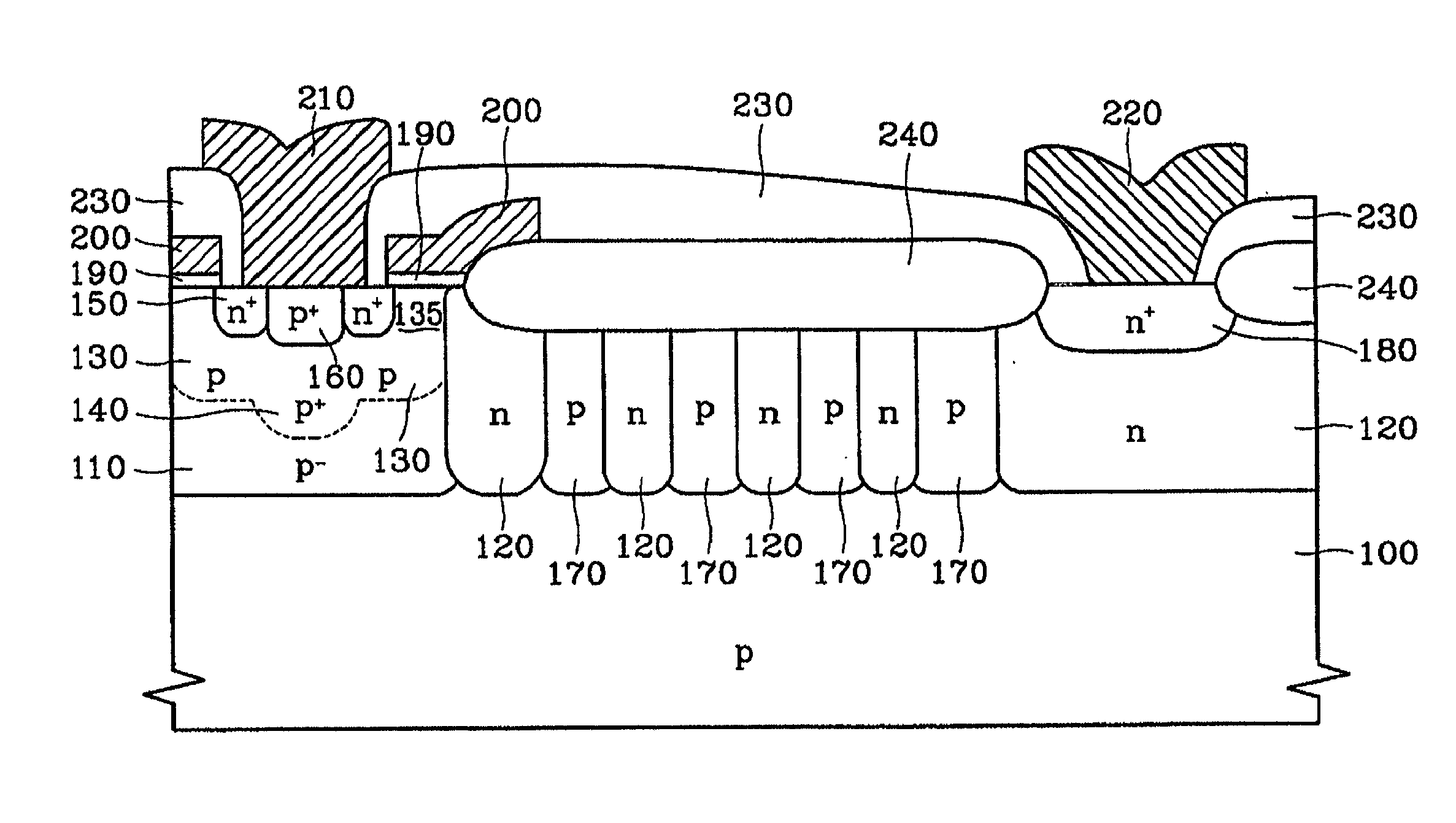
[0021] Referring to FIGS. 3 through 5, a p.sup.-well region 110 and an n.sup.- well region 120 are formed in the upper portion of a p-type semiconductor substrate 100. The p-well region 110 may be omitted. The n.sup.- well region 120 is used as a drift region. A p-body region 130 having a channel region 135 on its surface and a deep p.sup.+ body region 140 surrounded...


PUM


Abstract

A high voltage lateral Double diffused Metal Oxide Semiconductor (DMOS) transistor includes a plurality of well regions of a first conductivity type formed to be spaced out within a well region of a second conductivity type between a channel region of the first conductivity type and a drain region of the second conductivity type. Most current is carried through some portions of the well region of the second conductivity type in which the well regions of the first conductivity do not appear so that the current carrying performance of the device is improved. When a bias voltage is applied to the drain region, the well region of the second conductivity type is completely depleted at other portions where the well region of the second conductivity type and the well regions of the first conductivity type alternately appear so that the breakdown voltage of the device can be increased. In addition, since the well region of the second conductivity type can be easily depleted, not only the breakdown voltage can be increased, but also the impurity concentration of the well region of the second conductivity type can be increased. Accordingly, the on-resistance of the device can be decreased.

Description

REFERENCE TO RELATED APPLICATIONS[0001] This application claims priority of Korean patent application Serial No. 01-20168, filed Apr. 16, 2001.[0002] 1. Field of the Invention[0003] The present invention relates to a power semiconductor device, and more particularly, to a high voltage lateral Double diffused Metal Oxide Semiconductor (DMOS) transistor having low on-resistance and high breakdown voltage.[0004] 2. Description of the Related Art[0005] Integrated circuits in which a control function and a driver function are combined are usually referred to as smart power devices. Such a smart power device has a lateral DMOS transistor at its output terminal which is designed to usually operate with high voltage. In such a high voltage lateral DMOS transistor, breakdown voltage is critical in terms of the stability of a device, and on-resistance is critical in terms of the operational characteristics of the device. In order to decrease the on-resistance of the device, the doping concent...

Claims


Application Information

Patent Timeline
IPC IPC(8): H01L29/06H01L29/772H01L29/78
CPCH01L29/0634H01L29/7835H01L29/7801H01L29/7816H01L29/0692H01L29/42368H01L29/772
Inventor KIM, MIN-HWANJEON, CHANG-KICHOI, YOUNG-SUK
Owner SEMICON COMPONENTS IND LLC
Why Eureka
Try Eureka