Secure and static 4T SRAM cells in EDRAM technology

a sram cell, static technology, applied in the direction of digital storage, instruments, semiconductor devices, etc., can solve the problems of limited program execution speed of modern digital data processors, affecting the performance of memory cells, and affecting the degree to which any given memory cell design can be scaled to smaller sizes without compromising performan

Inactive Publication Date: 2004-02-19
IBM CORP
View PDF7 Cites 11 Cited by
  • Summary
  • Abstract
  • Description
  • Claims
  • Application Information

AI Technical Summary

Problems solved by technology

Modern digital data processors are often limited in program execution speed by the time required for memory access.
However, memory access time and the cost of storage varies widely with the storage medium.
However, it has been found that the degree to which any given memory cell design can be scaled to smaller sizes without compromising performance is often limited.
Perhaps more importantly at the current state of the art, memory cells become increasingly susceptible to soft errors due to ionization and charge injection caused by alpha particles impinging on the chip at or close to the memory cell.
It is generally considered that the soft error rate doubles with each new generation of memory device designs.
SRAM cells are particularly susceptible to soft errors since charge injection can cause the bistable circuit of the memory cell to switch or flip storage states.
The degree to which a SRAM cell can be physically reduced in size (regardless of any attendant compromise of stability or imposition of operational constraint) is principally limited by the number of transistors required and, to a lesser extent, by the density of connections which must be made in metal layers (particularly the first layer which minimizes connection length and capacitance) formed over the transistors on the chip.
Several attempts to design a four transistor (4T) SRAM cell have been attempted but have been less than fully successful to date.
However this size reduction and increased integration density is achieved only at the expense of several serious trade-offs.
First, this design is much more susceptible to soft errors than the corresponding 6T design; the resistance of which to soft errors at current minimum feature size regimes such as 0.13 micron and 0.09 micron minimum feature size ground rules is considered marginal although acceptable in some short term and non-critical storage applications such as for display screen memories.
Cells along the selected columns and unselected rows will be losing data since the static pull-up leakage current would be missing when the selected bit lines are switched toward ground.
Accordingly, these constraints have prevented this design approach from being applied to memory cells for general applications.

Method used


Image

  • Secure and static 4T SRAM cells in EDRAM technology
  • Secure and static 4T SRAM cells in EDRAM technology
  • Secure and static 4T SRAM cells in EDRAM technology

Examples


Embodiment Construction

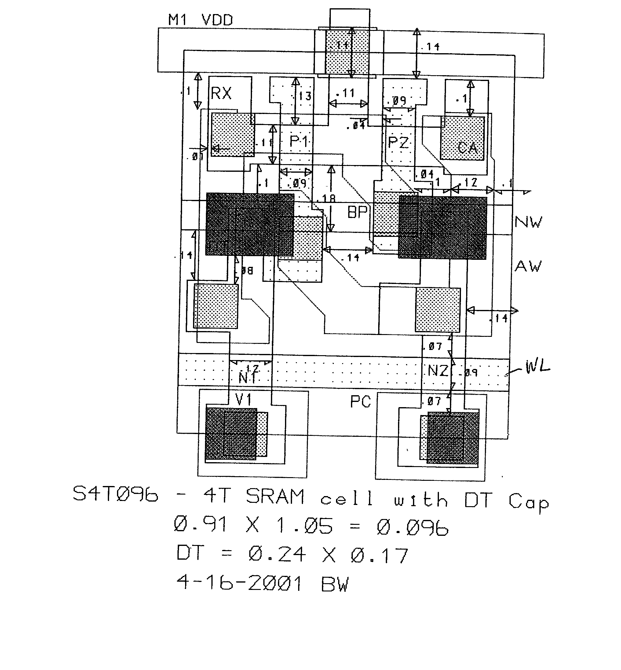
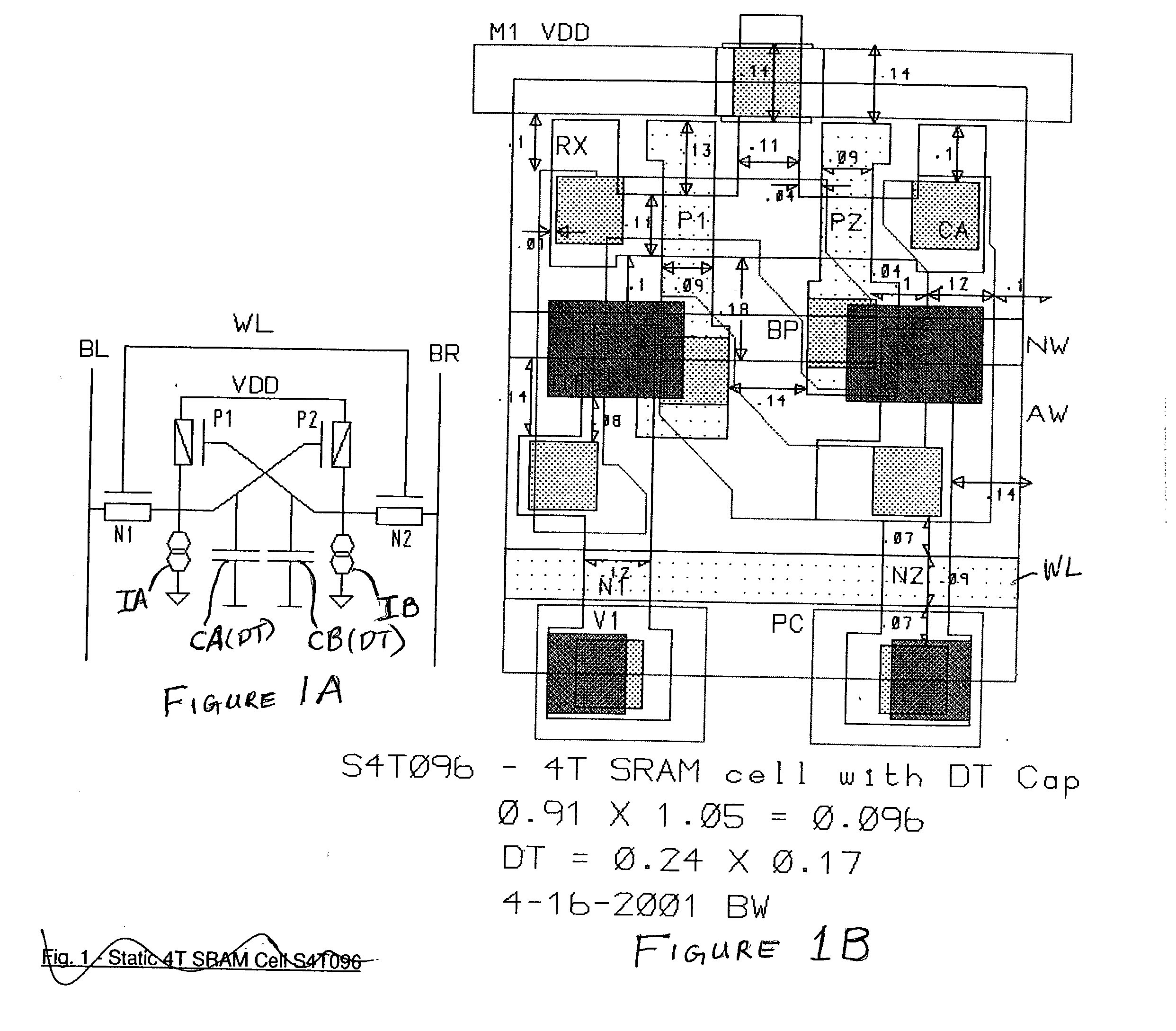
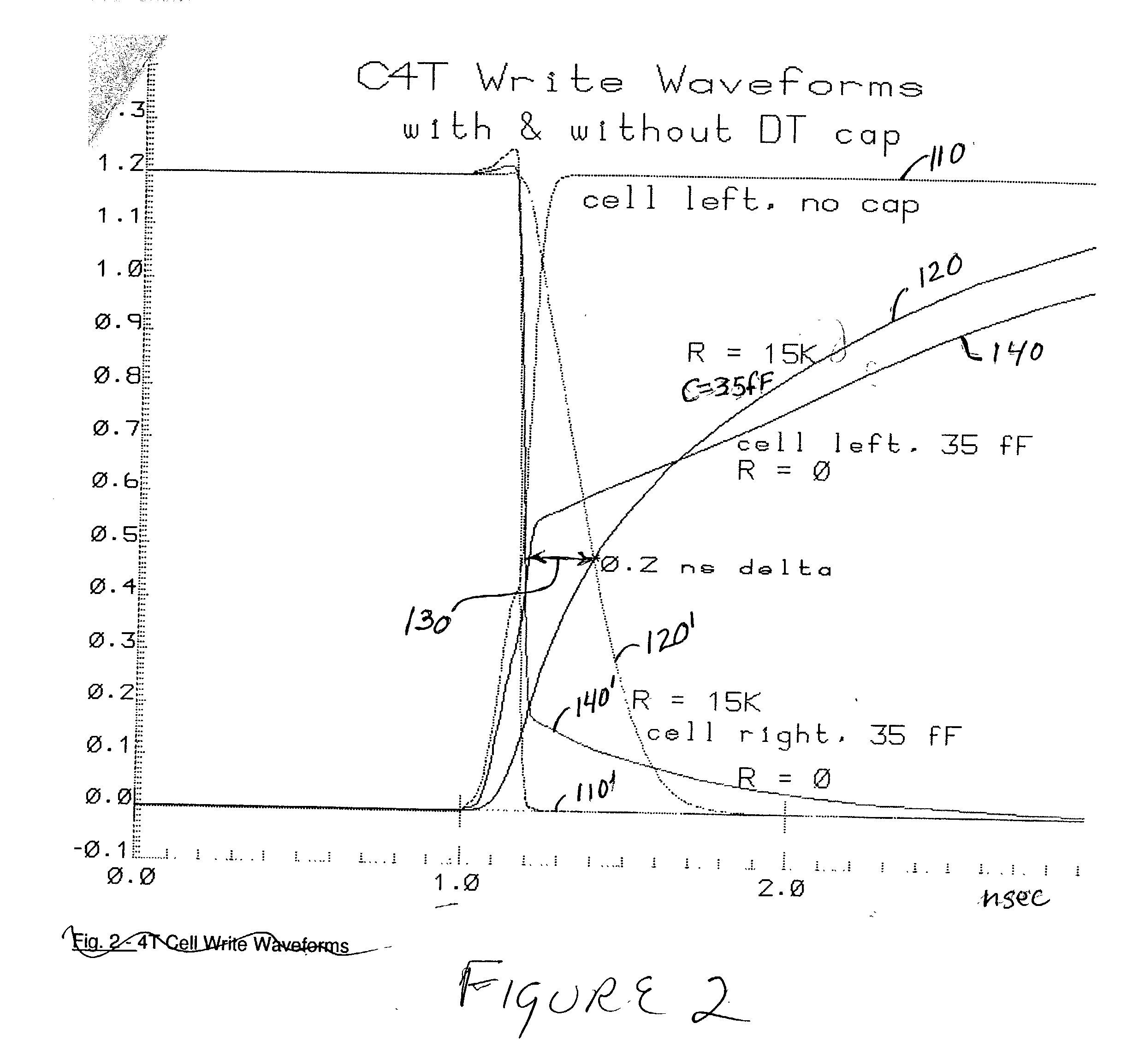
[0018] Referring now to the drawings, and more particularly to FIG. 1A, there is shown a schematic circuit diagram of a 4T memory cell in accordance with the invention. It will be appreciated by those skilled in the art from the following discussion that the present invention exploits several generally undesirable characteristics of various circuit elements which are increased as the elements are scaled to smaller sizes to provide a memory cell having fewer elements which nevertheless achieves enhanced stability without constraints on the mode of operation which conflict with or may be contrary to common modes of operation. These meritorious effects are achieved in accordance with the invention while improving soft error immunity or at least avoiding expected increases in soft error susceptibility.

[0019] More specifically, the invention principally uses a capacitor technology developed for so-called embedded DRAMs (EDRAM) which can be fabricated at extremely small size in a substrat...


PUM


Abstract

Disclosed herein is a 4T (four transistor) SRAM cells. Stability, fabrication and integration density advantages as well as a high degree of soft error immunity with small and potentially tailorable write delay penalty may potentially be available in a memory cell by providing a source of pull down current through leakage of stabilizing capacitors, pass gate transistor leakage / off current, or a combination thereof. The source of pull down current allows omission of active pull down devices in a four transistor memory cell circuit to substantially reduce memory cell size or footprint while providing levels of soft error immunity comparable to or exceeding that of known 6T memory cell designs fabricated at comparable minimum feature size regimes and avoiding the expected increase of soft error rates as minimum feature size and / or number of circuit elements is reduced.

Description

[0001] 1. Field of the Invention[0002] The present invention generally relates to digital memory cell circuits for high density integrated circuits and, more particularly, to memory circuits having reduced size with improved soft error immunity.[0003] 2. Description of the Prior Art[0004] Modern digital data processors are often limited in program execution speed by the time required for memory access. However, memory access time and the cost of storage varies widely with the storage medium. Therefore, various arrangements have come into widespread use which seek to provide a limited amount of memory in electronic storage, such as static or dynamic random access memories (RAM), which may be accessed very rapidly while larger storage is provided in, for example, magnetic media. Nevertheless, the demand for increased processing speed with reductions in the cost of electronic memory with increased integration density of integrated circuits has led to increased demands for more storage ...

Claims


Application Information

Patent Timeline
Patent Type & Authority Applications(United States)
IPC IPC(8): G11C11/412H01L27/11H01L27/12
CPCG11C11/412H01L27/1203H01L27/1104H10B10/12
Inventor WONG, ROBERT C.
Owner IBM CORP
Why Eureka
Try Eureka