
Method for selecting reference images, method and apparatus for inspecting patterns on wafers, and method for dividing a wafer into application regions

a technology of reference images and wafers, applied in image enhancement, semiconductor/solid-state device testing/measurement, instruments, etc., can solve the problems of lowering the sensitivity of defect detection, difficult to reduce process noise from semiconductor devices, and increasing the sensitivity requirements for appearance inspections

Inactive Publication Date: 2004-03-25
SAMSUNG ELECTRONICS CO LTD
View PDF6 Cites 83 Cited by
  • Summary
  • Abstract
  • Description
  • Claims
  • Application Information

AI Technical Summary

Problems solved by technology

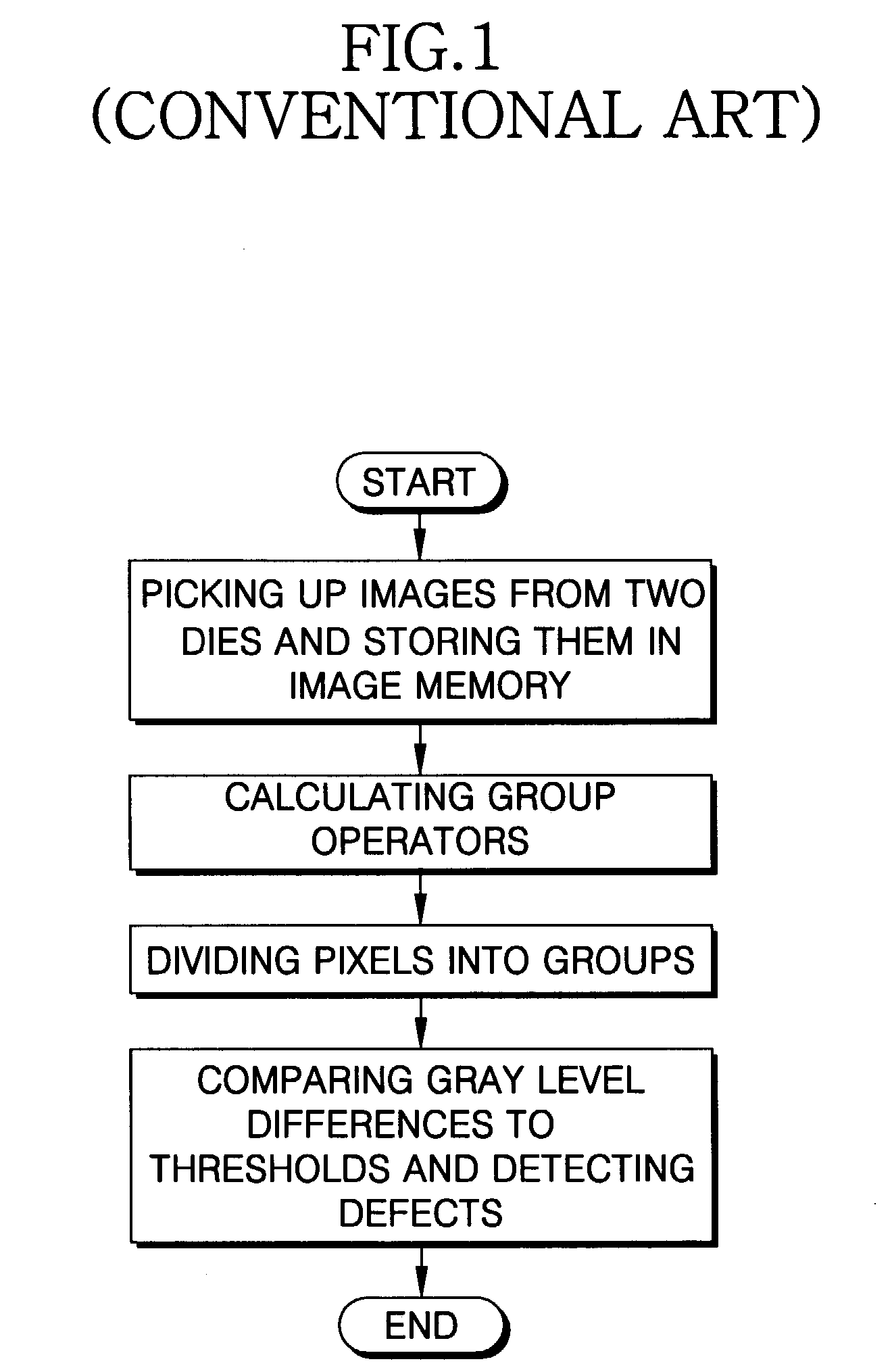
Recently, however, sensitivity requirements for appearance inspections have increased due to the design rules for semiconductor devices.
In practice, however, it is difficult to reduce process noise from semiconductor devices.
If a fixed threshold is applied to a region when checking the difference between the gray levels of two pixels and process noise is present, the process noise may be recognized as a defect, thereby lowering the defect detecting sensitivity.
Thus, since the process noise may be a minor defect, the process noise may not be detected.
Therefore, process noise such as the metal grain in the metal wires may not be detected as defects, and defects such as a short between circuit wires may be detected.
However, such a method for inspecting patterns may cause errors with respect to the determination of which dies are truly defective.
Thus, because of the difference in the gray levels of the central dies and the edge dies, edge dies having no defects may be improperly identified as defective dies.
Therefore, errors with respect to the determination of defective dies may occur when one image of a central die or on image of an edge die is used as the reference image and a pattern inspection is performed on all of the dies of the wafer.

Method used


Image

  • Method for selecting reference images, method and apparatus for inspecting patterns on wafers, and method for dividing a wafer into application regions
  • Method for selecting reference images, method and apparatus for inspecting patterns on wafers, and method for dividing a wafer into application regions
  • Method for selecting reference images, method and apparatus for inspecting patterns on wafers, and method for dividing a wafer into application regions

Examples


Embodiment Construction

[0040] Exemplary embodiments of the present invention will now be described more fully with reference to the accompanying drawings, in which exemplary embodiments of the invention are shown. This invention may, however, be embodied in many different forms and should not be construed as being limited to the exemplary embodiments set forth herein. Rather, these exemplary embodiments are provided so that this disclosure will be thorough and complete and will fully convey the concept of the invention to those skilled in the art. In the drawings, the thicknesses of layers and regions are exaggerated for clarity. It will also be understood that when an element is referred to as being "on" another layer or substrate, it may be located directly on the other element, or intervening elements may be present. It is to be further understood that when an element is referred to as being "between" two other elements, it may be positioned such that the two other elements contact the element, or inte...


PUM

PropertyMeasurementUnit
optical microscopeaaaaaaaaaa
thresholdaaaaaaaaaa
widthaaaaaaaaaa

Abstract

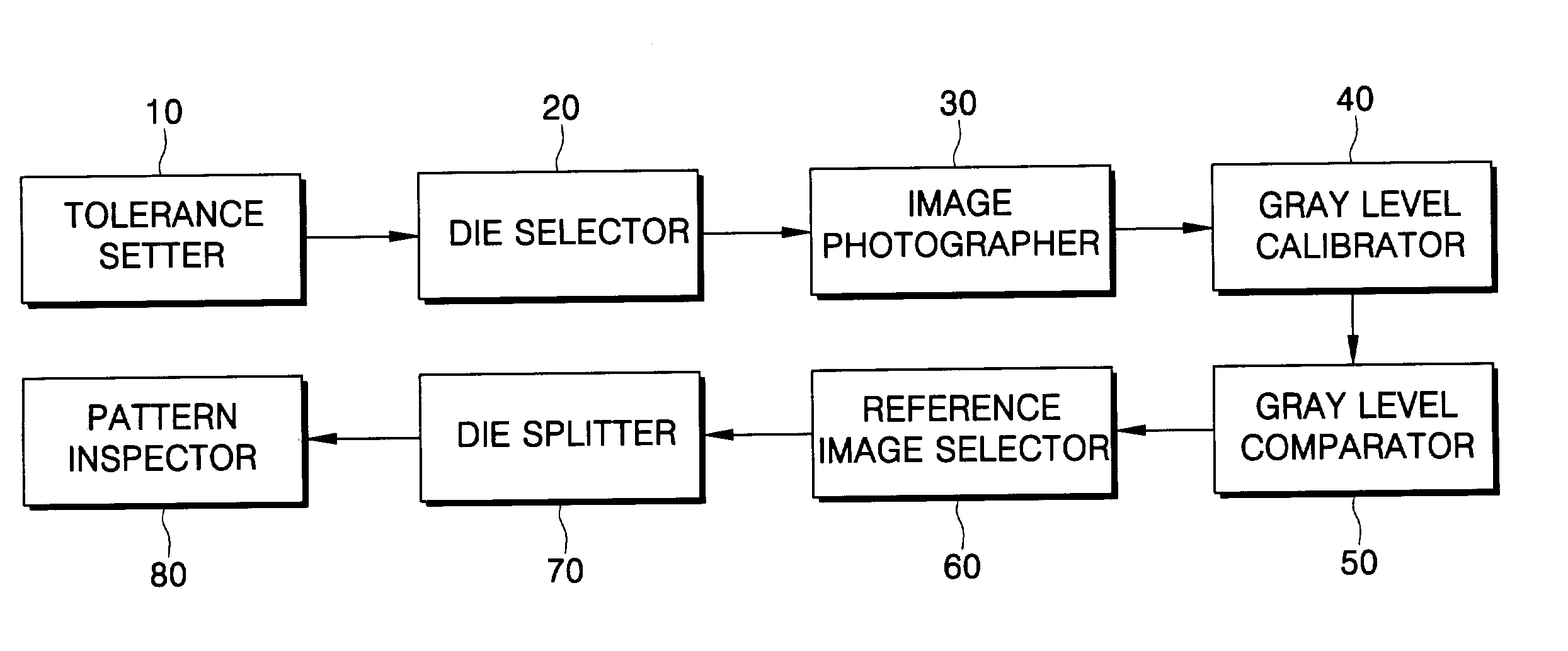
A method for selecting reference images, a method and an apparatus for inspecting patterns on a wafer, and a method for dividing a wafer into application regions. In a method for inspecting patterns according to at least one exemplary embodiment of the present invention, a plurality of reference dies may be selected and a difference in gray levels of images of the references dies may be determined. The reference dies may include a first die substantially centrally located on the wafer and at least one second die located at an edge portion of the wafer. One reference image is selected if the difference in gray levels is within a permitted tolerance and more than one reference image may be selected if the difference in gray levels is not within the permitted tolerance. A pattern inspection may be performed using the reference images.

Description

[0001] This U.S. non-provisional patent application claims priority under 35 U.S.C. .sctn.119 to Korean Patent Application 2002-57510, filed Sep. 23, 2002, the contents of which are incorporated by reference in their entirety.[0002] 1. Field of the Invention[0003] The present invention relates to a method for selecting reference images, a method and an apparatus for inspecting patterns on wafers, and a method for dividing a wafer into application regions, and more particularly to a method for selecting a plurality of reference images which may be used to perform pattern inspections in application regions on wafers which correspond to the reference images.[0004] 2. Description of the Related Art[0005] In a conventional apparatus for inspecting the appearance of semiconductor integrated devices, once the images of two adjacent semiconductor devices or dies are obtained, the images of the dies are compared to each other by a pixel unit. To determine if one of the dies is defective, the...

Claims


Application Information

Patent Timeline
Patent Type & Authority Applications(United States)
IPC IPC(8): H01L21/66G01N21/956G06T7/00
CPCG01N21/95607G03F7/7065G06T2207/30148G06T7/001G06T7/0002H01L22/00
Inventor LEE, BYOUNG-HOKIM, DEOK-YONG
Owner SAMSUNG ELECTRONICS CO LTD
Features
  • Generate Ideas
  • Intellectual Property
  • Life Sciences
  • Materials
  • Tech Scout
  • Unparalleled Data Quality
  • Higher Quality Content
  • 60% Fewer Hallucinations
Learn More