Circuit board having boundary scan self-testing function

a circuit board and self-testing technology, applied in the field of circuit boards having self-testing functions, can solve the problems of narrowing the line width, requiring more sophisticated electrical packaging, and complicated electronic devices, and traditional probe tests have encountered a tremendous handicap

Inactive Publication Date: 2004-04-08
LEADTEK
View PDF5 Cites 25 Cited by
  • Summary
  • Abstract
  • Description
  • Claims
  • Application Information

AI Technical Summary

Problems solved by technology

On the other hand, these requirements have made electronic devices more complicated, requiring more sophisticated electrical packaging and narrowing the line widths on circuit boards.
Therefore, the traditional probe test has encountered a tremendous handicap.
In order to overcome such challenges, the costs will inevitably go up.
For example, when the packaging type of devices is a flip-chip or BGA with more than 500 pins, the traditional probe is not adequate for testing such devices.
However, since the boundary scan testing still needs to be carried out by the ATE 15 away from the circuit board 10, the testing service fees are obviously high.
In addition, the CPLD 112 on the substrate 13 cannot effectively and simultaneously detect all errors.

Method used


Image

  • Circuit board having boundary scan self-testing function
  • Circuit board having boundary scan self-testing function
  • Circuit board having boundary scan self-testing function

Examples


Embodiment Construction

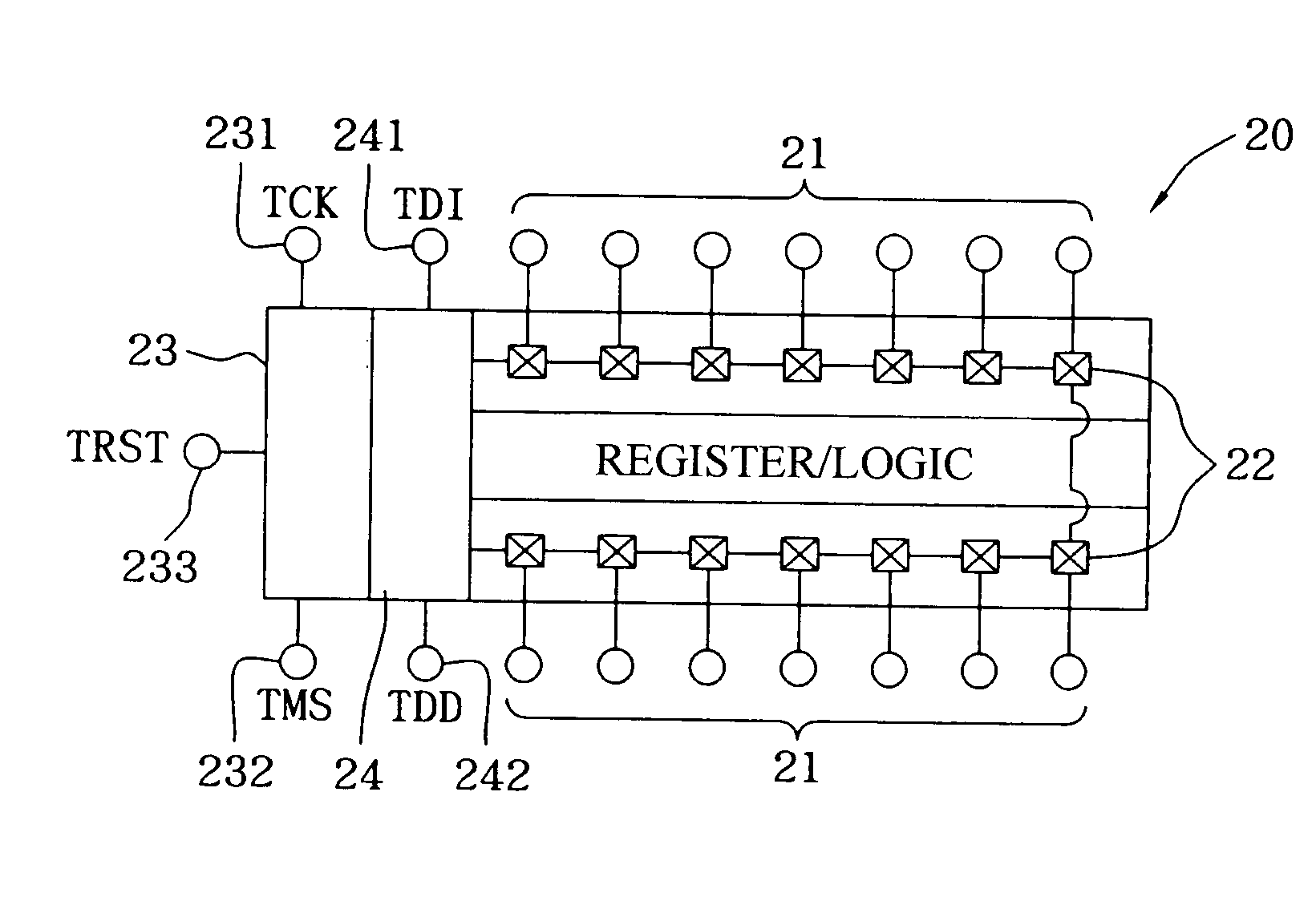
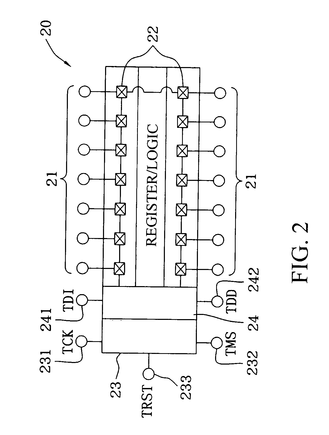
[0018] FIG. 2 is a schematic block diagram of the device with a boundary scan circuit. The device 20 has several functional pins 21 extending from both sides of it. The functional pins 21 are for the execution of the functions assigned by the device 20. Each of the functional pins 21 is connected to a boundary register cell 22 capable of inputting and outputting data. One of the boundary register cells 22 is a shift register that connects to the adjoining one, and all the boundary register cells 22 are in a series connection with each other to form a boundary register. TAPs (Test Access Ports) 23 are the core of the device 20, and has various functional pins designated as follows: TCK (Test Clock Input) 231, TMS (Test Mode Selector) 232, and TRST (Test Reset Input) 233. In addition, the functional pins of TDI (Test Data Input) 241 and TDO (Test Data Output) 242 are, respectively, an input terminal and an output terminal for testing signals for the device 20. These two pins are conne...


PUM


Abstract

A circuit board with a boundary scan self-testing function comprises a substrate, a plurality of devices under test and an active testing device. The active testing device mounted the substrate can conduct circuit testing on the plurality of devices under test, and self-testing is allowed without employing any external testing equipment. The testing data of the active testing device is transmitted through a predetermined test route on the circuit board. Each of the devices under test is completely tested of all designated functions in either series connection or parallel connection with each other. The testing can help find out whether the devices have any defects.

Description

[0001] 1. Field of the Invention[0002] The present invention relates to a circuit board having a boundary scan self-testing function, and more particularly to a circuit board capable of actively conducting circuit testing by its built-in self-testing function.[0003] 2. Description of the Related Art[0004] Boundary scan is a very successful testing method first developed by JTAG (Joint Test Action Group) during the 80 s. At the beginning, this testing method was developed for testing circuit boards or system levels, and has been widely accepted by the industry up until now. Boundary scan has become the standard IEEE 1149.1 that most IC designers have followed. This standard defines that specific testing circuits embedded in key IC devices on a circuit board can perform various chip-level tests at a board level.[0005] In recent years, the requirements of the consumer market have not only driven electronic products to have smaller sizes, such as phones and digital cameras, but also to ...

Claims


Application Information

Patent Timeline
Patent Type & Authority Applications(United States)
IPC IPC(8): G01R31/28H04L1/22
CPCG01R31/2815
Inventor LIU, MENG-HSIEN
Owner LEADTEK
Why Eureka
Try Eureka