Wide-viewing angle display device and fabrication method for thereof
- Summary
- Abstract
- Description
- Claims
- Application Information
AI Technical Summary
Problems solved by technology
Method used
Image

Examples
first embodiment
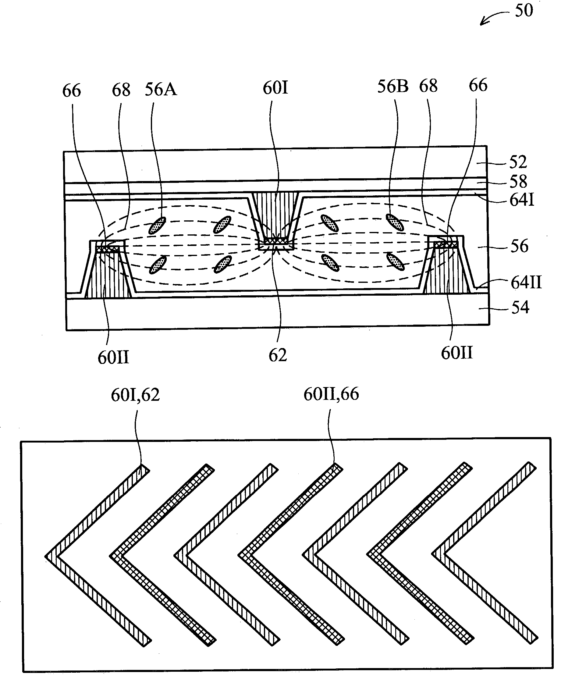
[0028] FIG. 3 is a sectional diagram illustrating an MVA mode LCD device according to the present invention. AN MVA mode LCD device 50 comprises an upper substrate 52 of transparent glass and a lower substrate 54 of transparent glass disposed parallel to each other, and an LC layer 56 is formed in a space therebetween. The upper glass substrate 52 serves as a CF (color filter) substrate, on which a black matrix layer 58 is partially overlapped with a plurality of color elements. Also, a plurality of first protrusions 60I is formed on the black matrix layer 58, and plurality of common electrodes 62 is formed on the tops of the first protrusions 60I, respectively. Moreover, a first alignment layer 64I is formed on the exposed surface of the black matrix layer 58, the first protrusions 60I and the common electrodes 62.
[0029] The lower substrate 54 serves as a TFT array substrate, on which a plurality of TFTs and an active matrix driving circuit are formed. Also, a plurality of second p...
second embodiment
[0034] FIG. 5 is a sectional diagram illustrating an MVA mode LCD device according to the second embodiment of the present invention. AN MVA mode LCD device 70 in the second embodiment is substantially similar to the MVA mode LCD device 50 of the first embodiment, with the similar portions omitted herein. Regarding the dissimilar portions, the fabrication of the first protrusion 60I is omitted from the upper substrate 52, and a plurality of first common electrodes 62I is formed on the black matrix layer 58 of the upper substrate 52. Also, a plurality of second common electrodes 62II is formed on the lower substrate 54 and in a position corresponding to the first common electrodes 62I. The first common electrodes 62 and the pixel electrodes 66 are arranged alternately, so that the second common electrode 62II and the pixel electrodes 66 are arranged alternately.
[0035] The pixel electrodes 66 are suspended in the LC cell gap, and the common electrodes 62I and 62II are formed on the su...
third embodiment
[0038] FIG. 6 is a sectional diagram illustrating an IPS mode LCD device according to the third embodiment of the present invention. An IPS mode LCD device 80 comprises an upper substrate of transparent glass and a lower substrate 84 of transparent glass disposed in parallel to each other, and an LC layer is formed in a space therebetween. The upper substrate 82 serves as a CF substrate, which comprises a black matrix layer 88 with a plurality of color elements formed on the inner surface of the upper substrate 82, and a first alignment layer 90I formed on the black matrix layer 88.
[0039] The lower substrate 84 serves as a TFT array substrate, which comprises a plurality of TFTs and an active matrix driving circuit. Also, a plurality of first protrusions 92I and a plurality of second protrusions 92II are arranged alternately on the inner surface of the lower substrate 84, a plurality of first electrodes 94I is formed on the tops of the first protrusions 92I respectively, and a plura...
PUM
 Abstract
Description
Claims
Application Information
 - R&D Engineer
- R&D Manager
- IP Professional
- Industry Leading Data Capabilities
- Powerful AI technology
- Patent DNA Extraction
Browse by: Latest US Patents, China's latest patents, Technical Efficacy Thesaurus, Application Domain, Technology Topic.
© 2024 PatSnap. All rights reserved.Legal|Privacy policy|Modern Slavery Act Transparency Statement|Sitemap