Integrated circuit package configuration incorporating shielded circuit element structure

a shielded circuit and integrated circuit technology, applied in semiconductor devices, printed inductances, semiconductor/solid-state device details, etc., can solve the problems of difficult to achieve such a high q with conventional on-chip spiral inductors, spiral inductors are susceptible to electromagnetic interference,

Inactive Publication Date: 2004-11-11
SILICON LAB INC
View PDF33 Cites 94 Cited by
  • Summary
  • Abstract
  • Description
  • Claims
  • Application Information

AI Technical Summary

Problems solved by technology

It is difficult to achieve such a high Q with conventional on-chip spiral inductors using the conductor and dielectric layer compositions and thicknesses which are typically encountered in traditional integrated circuit processes.
In addition, such spiral inductors are susceptible to electromagnetic interference from external sources of noise.

Method used


Image

  • Integrated circuit package configuration incorporating shielded circuit element structure
  • Integrated circuit package configuration incorporating shielded circuit element structure
  • Integrated circuit package configuration incorporating shielded circuit element structure

Examples


Embodiment Construction

)

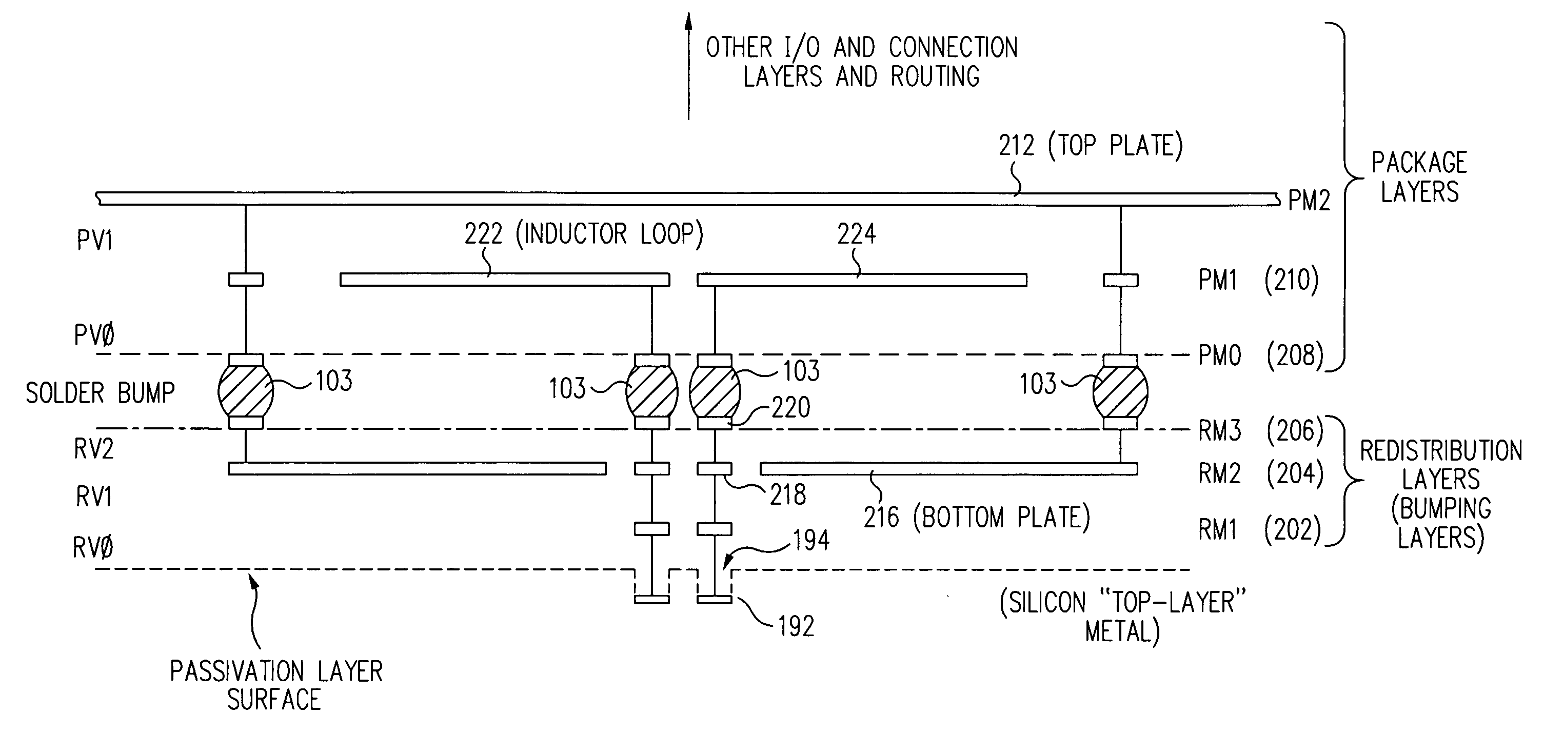
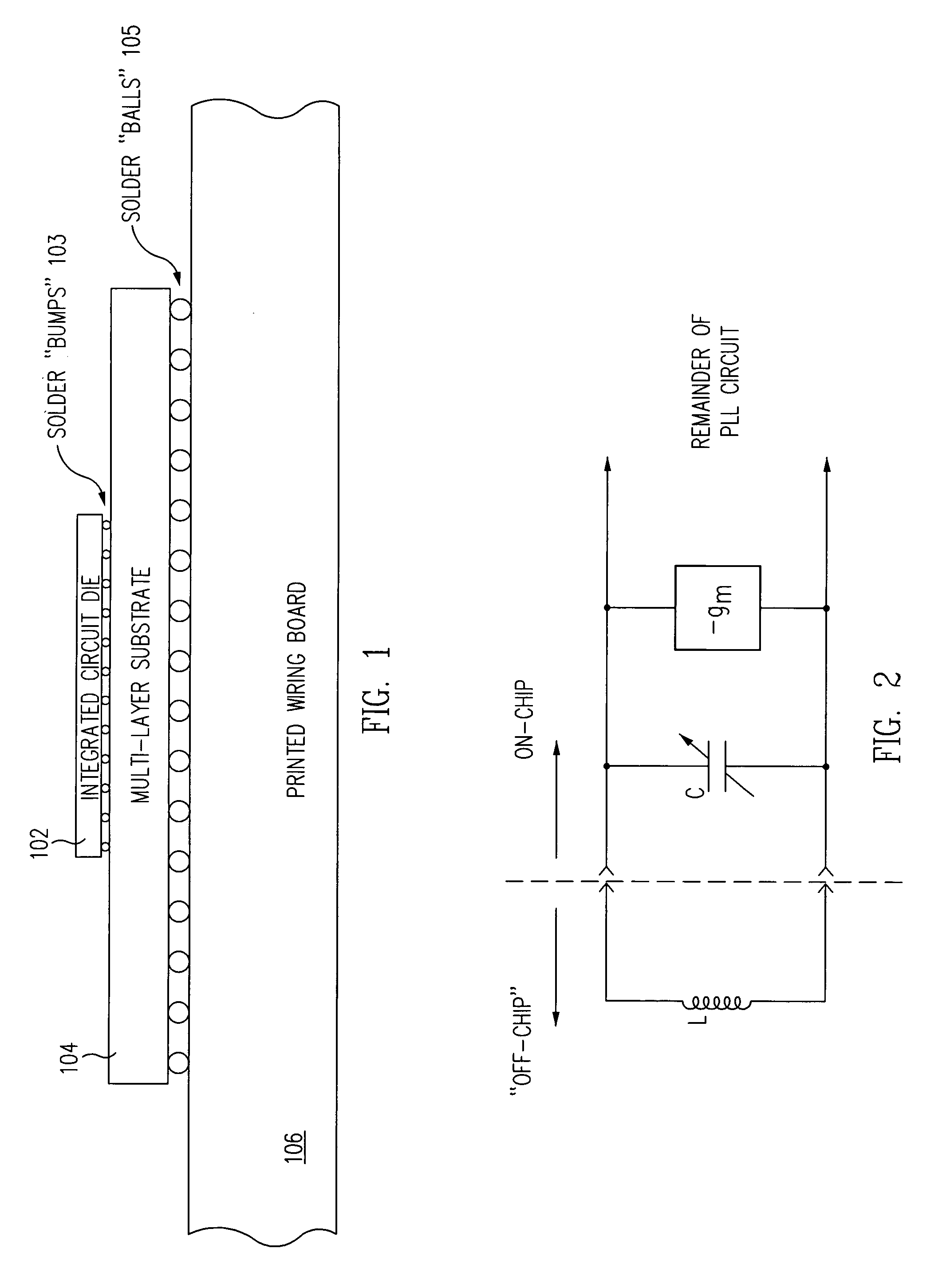
[0029] Referring now to FIG. 1, an integrated circuit die 102 is shown attached "top-side-down" (i.e., flip-chip) to a multi-layer substrate 104 using a plurality of solder "bumps" 103. Such solder bump technology is known in the art, and its use can provide a dense array of a large number of contacts to an integrated circuit die. The multi-layer substrate 104 is attached to a printed wiring board 106 using a plurality of solder "balls" 105. Such solder ball technology is known in the art, and package types which use such solder ball technology are frequently known as ball grid array (BGA) packages. The multi-layer substrate 104 is preferably a multi-layer ceramic substrate, although other types of substrate materials, such as fiberglass, may also be utilized.

[0030] In one embodiment of the invention, the integrated circuit die 102 may include a low-bandwidth phase locked loop (PLL) circuit as part of a clock regeneration device. The PLL includes an LC oscillator circuit. The capac...


PUM


Abstract

An electromagnetically-shielded high-Q inductor may be fabricated within a multi-layer package substrate (MLS). The inductor is preferably constructed as a loop structure on a layer of the MLS, and a shielding structure is formed around the inductor to substantially enclose the inductor in a Faraday cage-like enclosure. The shielding structure includes a top plate formed above the inductor on another layer of the MLS, and a bottom plate formed on yet another layer of the MLS or on a layer of an integrated circuit die which is below and attached to the MLS, preferably using solder bumps. Shielding structure sidewalls may be formed by a ring of stacked vias or via channels. The inductor is preferably connected to stacked vias which provide a connection to the underlying integrated circuit die by way of additional solder bumps and cut-outs through the bottom plate of the shielding structure.

Description

CROSS-REFERENCE TO RELATED APPLICATION(S)[0001] This application claims the benefit under 35 U.S.C. .sctn. 119(e) of U.S. Provisional Application No. 60 / 418,546, filed Oct. 15, 2002, entitled "INTEGRATED CIRCUIT PACKAGE CONFIGURATION INCORPORATING SHIELDED INDUCTOR STRUCTURE", naming Derrick C. Wei, Ying Shi, Kevin G. Smith, Steven P. Proffitt, Axel Thomsen and David M. Pietruszynski as inventors, which is hereby incorporated by reference.[0002] 1. Field of the Invention[0003] The present invention relates to integrated circuits incorporating shielded circuit structures, and more particularly to such integrated circuits incorporating inductor structures.[0004] 2. Description of the Related Art[0005] Many modern integrated circuit devices require extremely stable oscillators to achieve desired specifications. Crystal oscillators may be employed, but typically require an off-chip crystal mounted elsewhere on a printed-wiring-board. LC oscillators offer the potential advantage of being...

Claims


Application Information

Patent Timeline
Patent Type & Authority Applications(United States)
IPC IPC(8): H01L23/552H01L23/64
CPCH01F2017/008H01L23/552H01L23/645H01L2224/16H01L2924/01079H01L2924/15311H01L2924/3025H01L2224/16225H01L2924/00014H01L2224/0401
Inventor WEI, DERRICK C.SHI, YINGSMITH, KEVIN G.PROFFITT, STEVEN P.THOMSEN, AXELPIETRUSZYNSKI, DAVID M.
Owner SILICON LAB INC
Why Eureka
Try Eureka