Electronic component-built-in module

a technology of electronic components and modules, applied in the direction of sustainable manufacturing/processing, final product manufacturing, semiconductor/solid-state device details, etc., can solve the problems of unsuitable modules for reducing the size of electronic devices, destroying functions, and difficult to fill clearances

Active Publication Date: 2005-01-20
PANASONIC CORP
View PDF2 Cites 93 Cited by
  • Summary
  • Abstract
  • Description
  • Claims
  • Application Information

AI Technical Summary

Problems solved by technology

The mounting with bonding wires requires a larger area than that of electronic component 104 for joining with wires, thus making the module unsuitable for reducing the size of electronic devices.
Consequently, the solder causes short-circuiting failure between electrodes 1

Method used


Image

  • Electronic component-built-in module
  • Electronic component-built-in module
  • Electronic component-built-in module

Examples


exemplary embodiment 1

[0035] Exemplary Embodiment 1

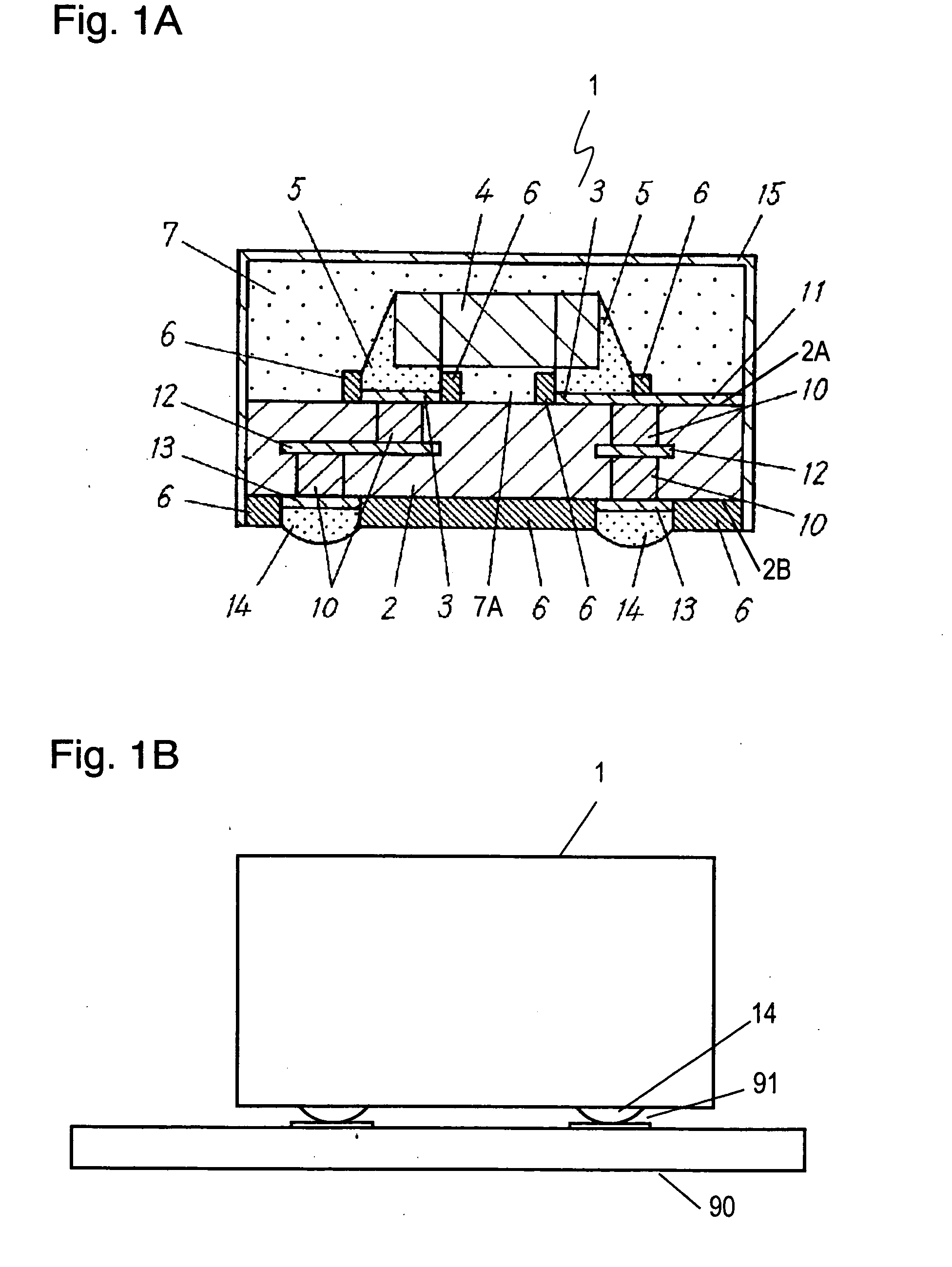
[0036]FIG. 1A is a sectional view of module 1 with built-in electronic component 4 accommodated therein according to Exemplary Embodiment 1 of the present invention. Multi-layered wiring board 2 includes electrode 3 and wiring pattern 11 on surface 2A, and includes wiring pattern 12 and inner via 10 inside of wiring board 2. Backside 2B has backside electrode 13 solder resist 6 thereon.

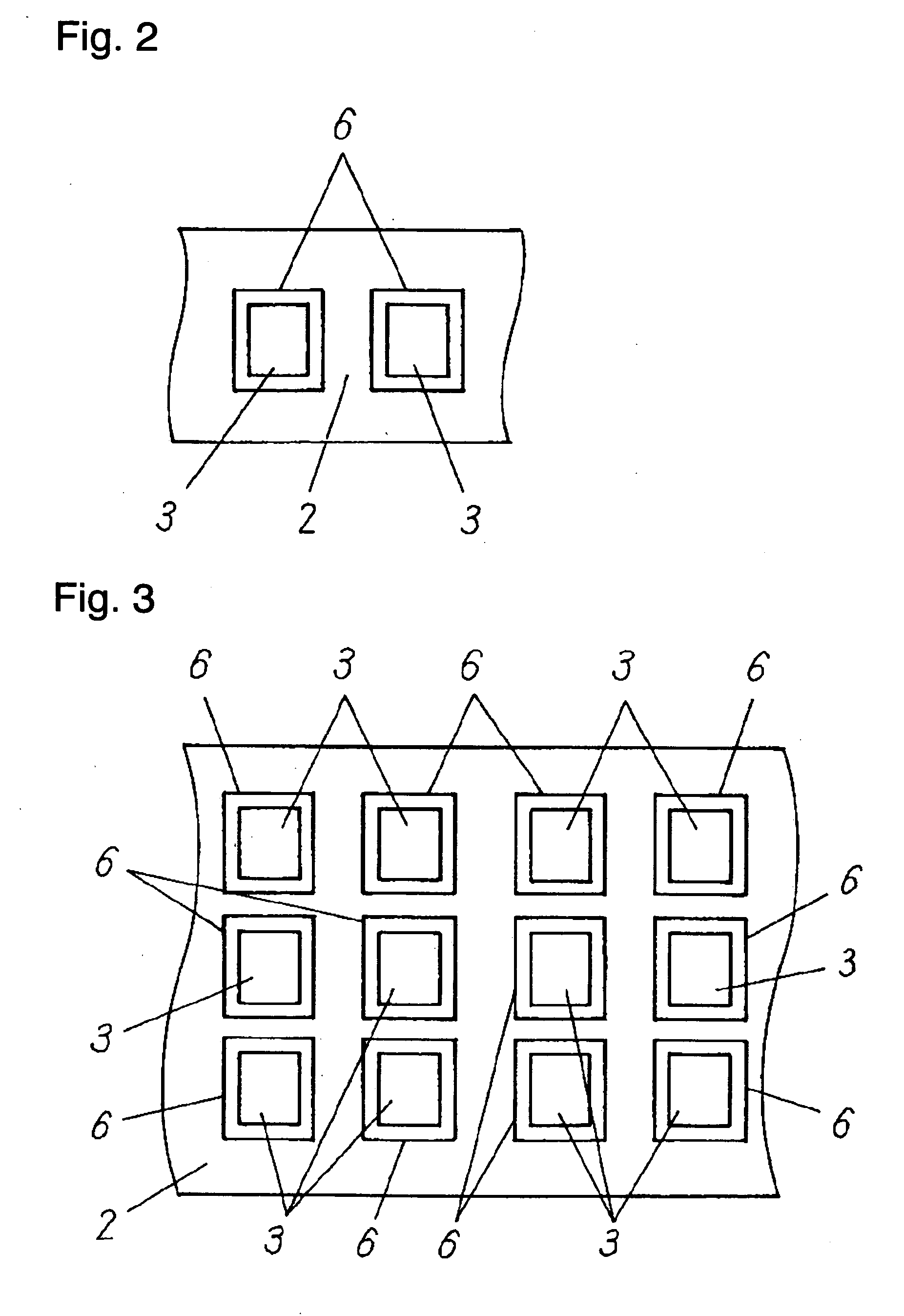
[0037]FIG. 2 is a top view of two electrodes 3 to be connected to electronic component 4 and the periphery of electrodes 3 on wiring board 2. Electrode 3 on surface 2A of wiring board 2 is surrounded by solder resist 6. Solder resist 6 is formed only around electrode 3. Solder resists 6 around electrodes 3 adjacent to each other are separated from each other and are not connected to each other at the bottom of electronic component 4, hence making a sufficient clearance between electronic component 4 and wiring board 2. Consequently, the clearance between electronic compon...

exemplary embodiment 2

[0049] Exemplary Embodiment 2

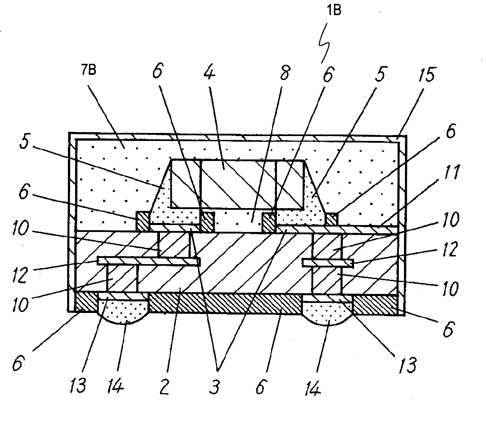
[0050]FIG. 4 is a sectional view of module 1B with built-in electronic component 4 according to Exemplary Embodiment 2 of the present invention. The same elements as those of Embodiment 1 are denoted by the same reference numerals and are not described in detail. Insulating resin 7B is formed around electronic component 4 and is made of material similar to that of insulating resin 7 shown in FIG. 1A according to Embodiment 1. As shown in FIG. 4, similarly to Embodiment 1, solder resist 6 is formed only around electrode 3, hence providing a large clearance between electronic component 4 and wiring board. The clearance between electronic component 4 and wiring board 2 is filled with insulating resin 8, and then, electronic component 4, insulating resin 8, and insulating resin 7B for covering wiring board 2 are provided. Then, metal film 15 functioning as an electromagnetic shield is formed on the surface of insulating resin 7B.

[0051] Insulating resin 8 is...

exemplary embodiment 3

[0055] Exemplary Embodiment 3

[0056]FIG. 5 is a sectional view of module 1C with the built-in electronic component according to Exemplary Embodiment 3 of the present invention. FIG. 6 is a top view of wiring board 2C of module 1C according to Embodiment 3. FIG. 7 is a sectional view of another module 1D according to Embodiment 3, and FIG. 8 is a top view of wiring board 2D of module 1D according to Embodiment 3. The same elements as those of Embodiment 1 are denoted by the same reference numerals and are not described detail.

[0057] As shown in FIGS. 5 and 6, similarly to Embodiment 1, in module 1C, solder resists 6 and 6C are formed only around electrodes 3 on the surface of wiring board 2C. Electronic component 4 is mounted with solder 5, and electronic component 24 is mounted with solder 25.

[0058] Electronic component 24 is a surface-mounted, active component including a semiconductor device, such as a transistor, IC, and LSI. Similarly to Embodiment 1, insulating resin 7 having ...


PUM


Abstract

A module includes an electronic component having at least two electrodes, a board having electrodes on its surface to be connected to the electrodes of the electronic component, respectively, solders for connecting the electrodes of the electronic component to the electrodes of the board, respectively, an insulating resin covering the electronic component, the surface of the board, the solder, and the electrodes, and solder resists provided on the surface of the board and around the electrodes of the board, respectively. One of the solder resists is separated from the other electrode at a portion between the electronic component and the board. When this module is mounted on a motherboard, the solder does not flow out of the electrodes even when the solder in the insulating resin melts.

Description

TECHNICAL FIELD [0001] The present invention relates to a module accommodating an electronic component, and more particularly to a module including a wiring board, electronic components arranged on an upper surface of the board, and an insulating resin for covering the electronic components. BACKGROUND ART [0002] Recently, small electronic devices are widely used which devices include a module with built-in electronic components which includes a board, plural electronic components arranged on the board, and a resin mold for covering the electronic components. FIG. 17 is a sectional view of conventional module 101 with a electronic component molded with resin. Wiring board 102 has a surface having wiring pattern 111 and electrode 103 thereon, and the surface is covered with solder resist 106. Wiring board 102 has inner via 110 electrically connecting wiring pattern 112 and backside electrode 113 formed on the backside of wiring board 102. Backside electrode 113 is provided with solde...

Claims


Application Information

Patent Timeline
IPC IPC(8): H01L21/60H05K3/28H05K3/34
CPCH01L24/16H01L2224/10175H01L2224/13099H01L2224/81801H01L2924/01004H01L2924/01013H01L2924/01015H01L2924/01022H01L2924/01027H01L2924/01029H01L2924/0103H01L2924/01039H01L2924/01074H01L2924/01075H01L2924/01078H01L2924/01079H01L2924/01082H01L2924/01322H01L2924/14H01L2924/15174H01L2924/15311H01L2924/19041H01L2924/19042H01L2924/19105H01L2924/3025H05K3/284H05K3/3436H05K3/3442H05K3/3452H05K2201/0209H05K2201/09909H05K2201/10636H05K2201/10674H05K2201/2036H01L24/81H01L2224/81136H01L2224/131H01L2924/014H01L2924/0105H01L2924/01047H01L2924/01033H01L2924/01024H01L2924/01021H01L2924/01019H01L2924/01006H01L2224/16225H01L2224/32225H01L2224/73204H01L2924/01005H01L2924/00H01L2224/05568H01L2224/05573H01L2224/06131H01L2224/26175H01L2924/00014Y02P70/50H01L2224/05599
Inventor KAWAMOTO, EIJIHAYAMA, MASAAKIKATSUMATA, MASAAKIYABE, HIROKI
Owner PANASONIC CORP
Why Eureka
Try Eureka