Multiple stacked-chip packaging structure

a packaging structure and chip technology, applied in semiconductor devices, semiconductor/solid-state device details, electrical devices, etc., can solve the problems of wire damage, failure of the whole packaging body, and inability to place the middle type or mixed type chip

Active Publication Date: 2005-02-17
ASE ASSEMBLY & TEST SHANGHAI +1
View PDF7 Cites 13 Cited by
  • Summary
  • Abstract
  • Description
  • Claims
  • Application Information

AI Technical Summary

Benefits of technology

[0008] The main and first object of the invention is to provide a multiple stacked-chip packaging structure, which can be designed freely and thus will not be limited by the layout patterns of bonding pads on the chip so that the middle type or mixed type chip can be placed on the upper layer or lower layer of the structure and the wires on the lower layer chip will not be impaired.
[0009] The second object of the invention is to provide a multiple stacked-chip packaging structure, which employs the design of carrier cap to ensure the degree of coplanar when performing wire bonding on the upper layer chip so as to facilitate the wire bonding process. By such design, the conventional problem that the degree of coplanar of nonconductive adhesive layer is not easy to be controlled can be resolved, and the fixed space between the upper layer and the lower layer can be maintained so as to protect the wires on the lower layer chip.
[0010] The third object of the invention is to provide a multiple stacked-chip packaging structure, which can provide a better way for heat dissipating so as to enhance heat-dissipating capability of the overall packaging structure.
[0011] The fourth object of the invention is to provide a multiple stacked-chip packaging structure, which incorporates the conventional wire-bonding process into the present sophisticated technique for manufacturing; therefore, it can reduce the process cost effectively.

Problems solved by technology

When the wire bonding of multiple stacked-chip packaging is performed, it is quite impossible to place the middle type or mixed type chip on the lower layer with the conventional wire bonding technique because the upper layer chip will result in wire damage on the lower layer chip.
Or, worse still, an open or short circuit of the wire can be resulted in, which eventually will fail the whole packaging body.
However, when the above method is in practice, a problem may occur; that is, a technique that is able to perform wire bonding at one side and not to impair wires at the other side is required during the operation.
Unfortunately, the conventional processing technique is hard to achieve the required technique.
Therefore, the method is problematic in real practice.
However, the degree of coplanar of a thicker nonconductive adhesive layer 48 is not easy to be controlled.
Therefore, the wire bonding process of the upper layer chip 50 will be difficult.
Yet, another problem may follow; that is, the lower layer wires may be impaired and therefore an open or short circuit problem may be resulted in since the nonconductive adhesive layer 48 will be softened and flattened during a subsequent high-temperature processing such as a reflow.
Therefore, the method is not easy to be implemented, either.

Method used


Image

  • Multiple stacked-chip packaging structure
  • Multiple stacked-chip packaging structure
  • Multiple stacked-chip packaging structure

Examples


Embodiment Construction

[0020] The invention utilizes a design of carrier cap to achieve an effect of multiple stacked-chip and not to be limited by the layout patterns of bonding pads on the chip so that the needed chips can be placed on the structure of upper layer or lower layer according to the requirement. Besides, the heat-dissipating effect can be increased, and the process cost can be lowered as well.

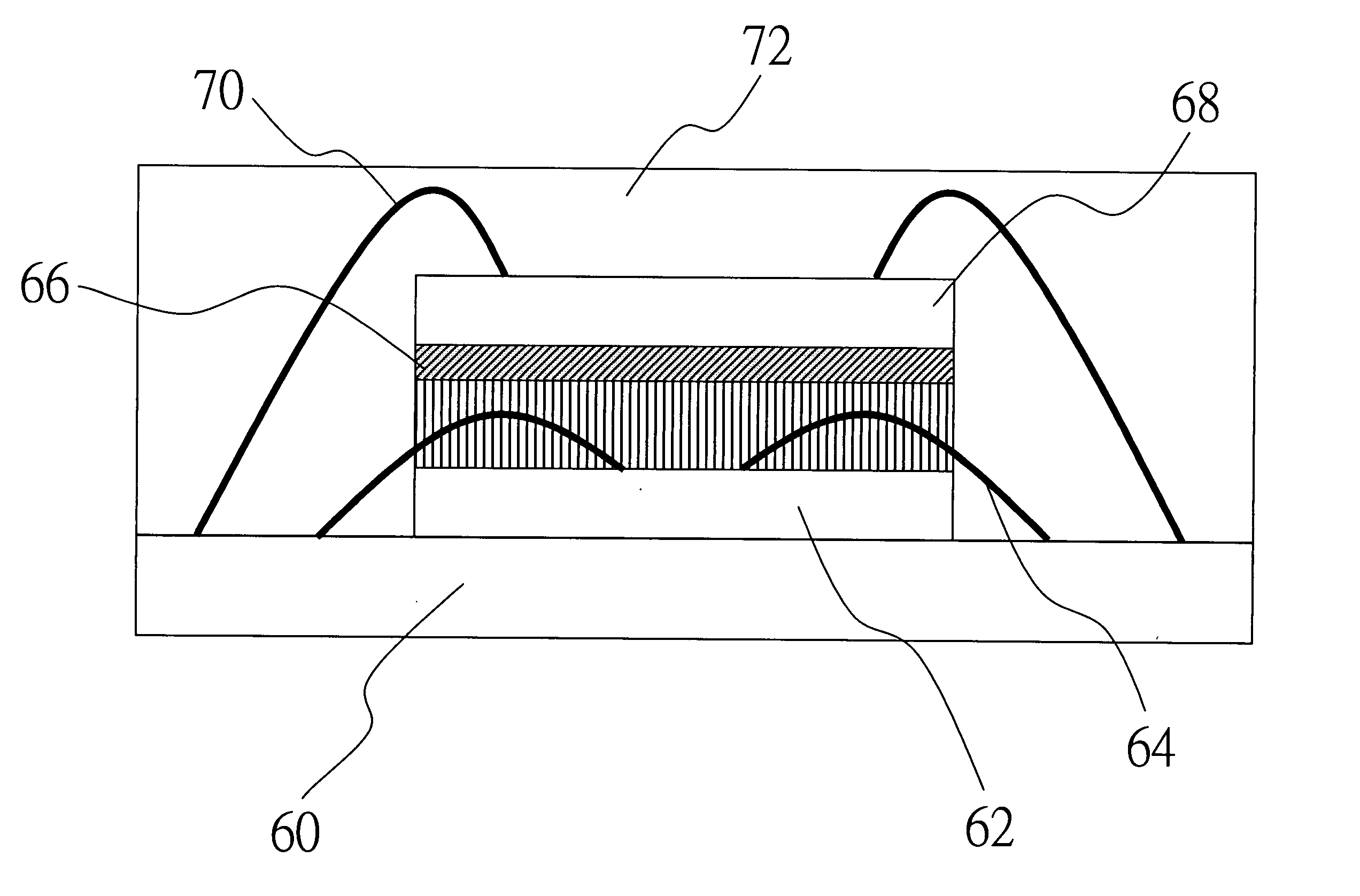
[0021] Referring to FIGS. 4 and 5, a multiple stacked-chip packaging structure is first to provide a middle-type lower layer chip 62 on a substrate 60, and then a plurality of wires 64 are electrically connected to the bonding pads 622 on the lower layer chip 62 and to the substrate 60. Next, a n-shaped carrier cap 66 is provided on the lower layer chip 62, wherein the n-shaped carrier cap 66 is made of thermal conductive material, and the height of n-shaped carrier cap 66 is taller than that of the wires 64 on the lower layer chip 62. Additionally, the n-shaped carrier cap 66 is detached from the bon...


PUM


Abstract

The invention provides a multiple stacked-chip packaging structure, including: at least one lower layer chip located on a substrate, wherein a plurality of wires are electrically connected to the bonding pads on the lower layer chip and to the substrate; at least one carrier cap provided on the lower layer chip to provide an accommodating space to the bonding pads and the wires on the lower layer chip; at least one upper layer chip provided on the carrier cap, wherein a plurality of wires are electrically connected to the bonding pads on the upper layer chip and to the substrate; and finally, a Molding Compound used to wrap up the foregoing components. The advantages of the invention are that the invention is not limited by the layout patterns of bonding pads on the chip, that the needed chips can be placed on either the upper layer or the lower layer structure according to the requirement, and that the degree of coplanar can be ensured when performing wire bonding on the upper layer chip so as to facilitate the wire bonding process.

Description

BACKGROUND OF THE INVENTION [0001] 1. Field of the Invention [0002] The invention relates to a multiple stacked-chip packaging structure and, more particularly, to a multiple stacked-chip packaging structure that is not subject to the layout patterns of bonding pads on the chip and is capable of protecting the lower chip and wires. [0003] 2. Description of the Related Art [0004] As shown from FIG. 1A to FIG. 1C, the layout patterns of bonding pads 12, 16&20 on chips 10, 14&18 respectively are generally divided into three categories: peripheral type, middle type, and mixed type. When the wire bonding of multiple stacked-chip packaging is performed, it is quite impossible to place the middle type or mixed type chip on the lower layer with the conventional wire bonding technique because the upper layer chip will result in wire damage on the lower layer chip. Or, worse still, an open or short circuit of the wire can be resulted in, which eventually will fail the whole packaging body. [0...

Claims


Application Information

Patent Timeline
Patent Type & Authority Applications(United States)
IPC IPC(8): H01L23/31H01L25/065
CPCH01L23/3121H01L24/33H01L2924/01033H01L24/48H01L2225/06589H01L2225/06575H01L2225/0651H01L25/0657H01L2224/32145H01L2224/48091H01L2224/48227H01L2224/73265H01L2924/00014H01L2924/00012H01L2924/181H01L24/73H01L2224/05553H01L2224/4824H01L2224/45099H01L2224/45015H01L2924/207
Inventor WU, WAN HUAWU, KAI CHIANG
Owner ASE ASSEMBLY & TEST SHANGHAI
Why Eureka
Try Eureka