Support structure for thinning semiconductor substrates and thinning methods employing the support structure

a technology of support structure and semiconductor substrate, which is applied in the direction of photomechanical equipment, instruments, and wellbore/well accessories, etc., can solve the problems of reducing robustness, pliable, and prone to sagging of semiconductor substrates, and reducing the robustness of semiconductor substrates

Active Publication Date: 2005-03-24
MICRON TECH INC
View PDF79 Cites 69 Cited by
  • Summary
  • Abstract
  • Description
  • Claims
  • Application Information

AI Technical Summary

Benefits of technology

[0010] The present invention includes a support structure, or carrier, for semiconductor substrates. The support structure is configured to be disposed upon an a

Problems solved by technology

When the thickness of a semiconductor substrate is reduced, however, the semiconductor substrate becomes less robust.
For example, when the thickness of a 200 mm diameter silicon wafer is reduced to about 230 μm or less, it becomes pliable and is prone to sagging when positioned on an edge or when an edge thereof is handled.
As a consequence of the reduced robustness of thinned semiconductor substrates, the semiconductor devices that have been fabricated thereon a

Method used


Image

  • Support structure for thinning semiconductor substrates and thinning methods employing the support structure
  • Support structure for thinning semiconductor substrates and thinning methods employing the support structure
  • Support structure for thinning semiconductor substrates and thinning methods employing the support structure

Examples


Embodiment Construction

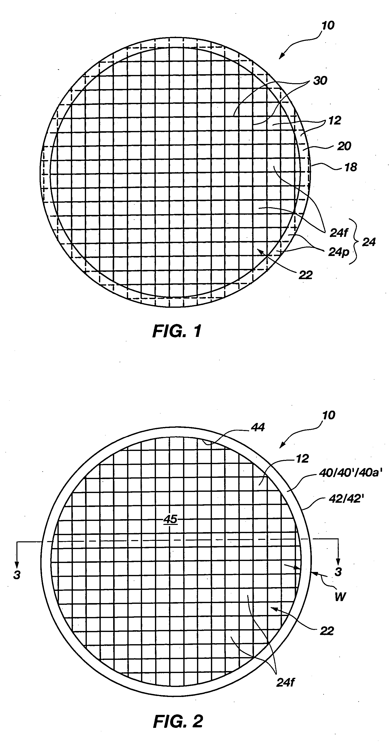
[0035] An example of a semiconductor substrate 10 is shown in FIG. 1. As illustrated, semiconductor substrate 10 may comprise a wafer of a semiconductor material, such as silicon, gallium arsenide, or indium phosphide.

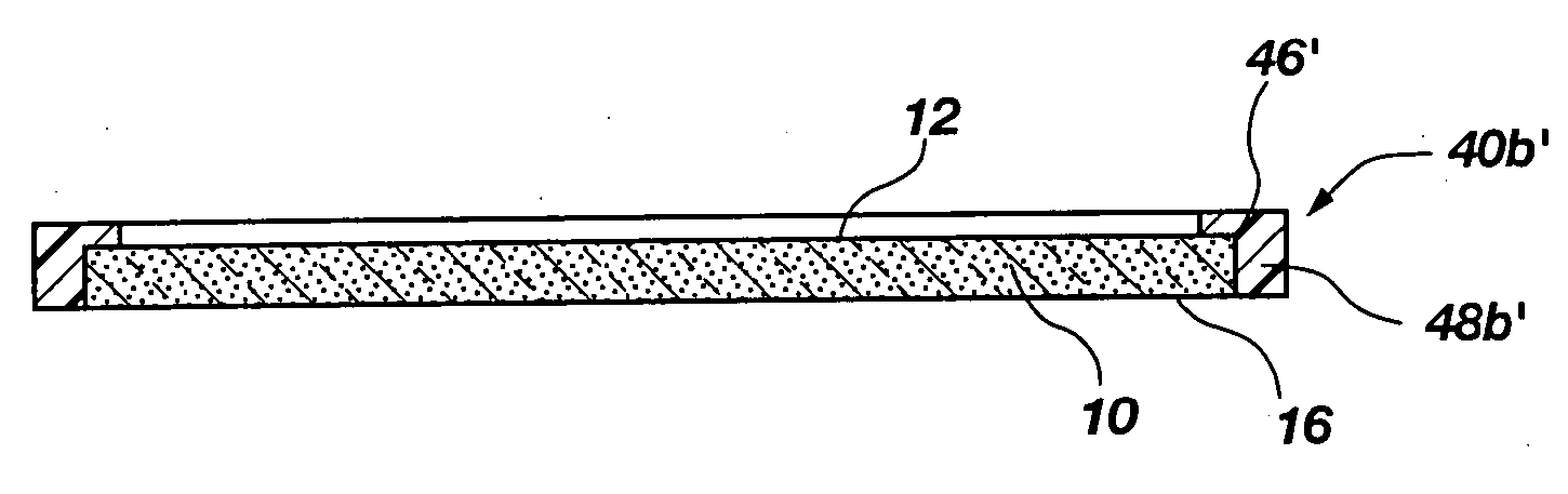
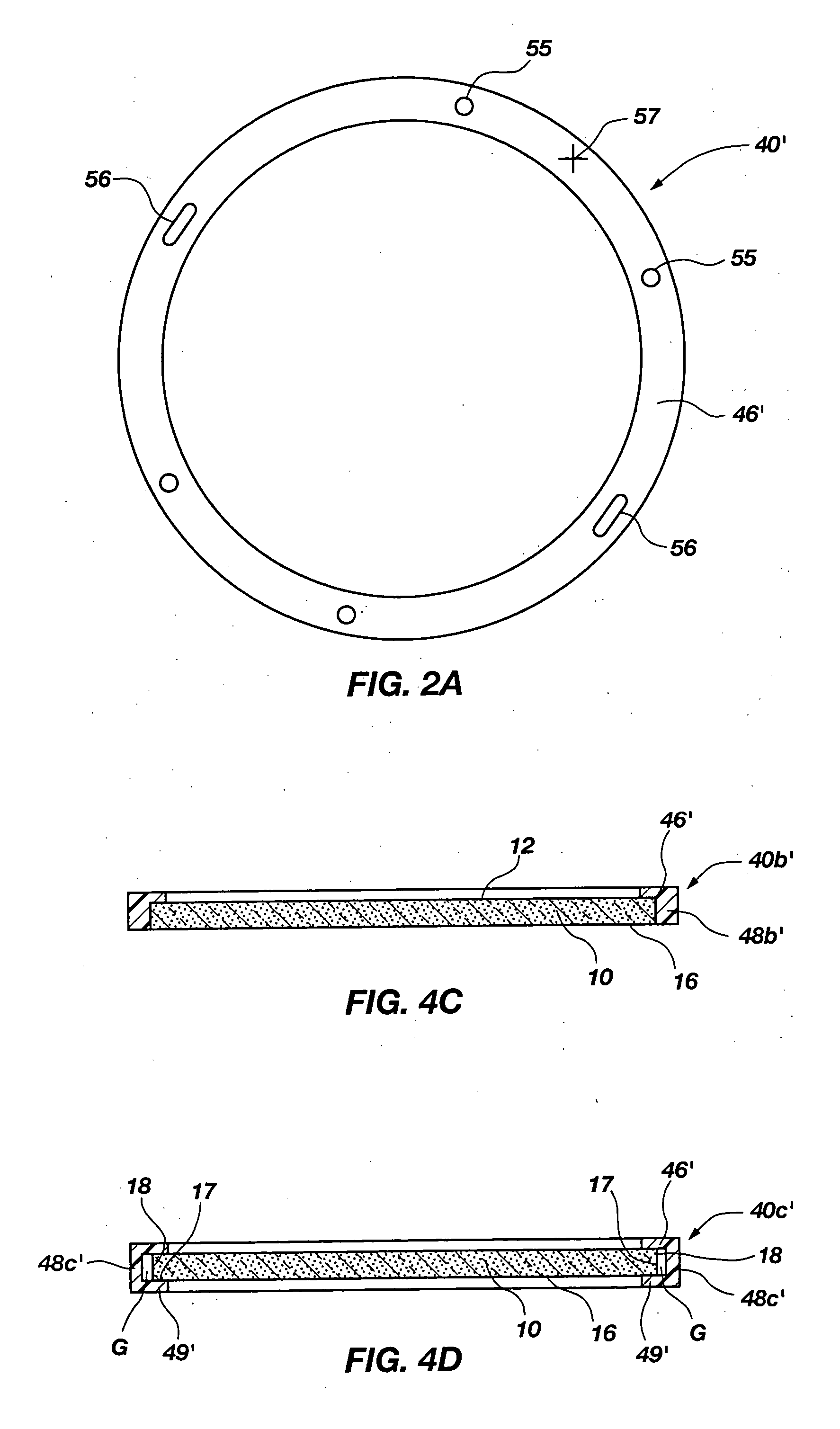
[0036] Semiconductor substrate 10 includes two opposite major surfaces, one of which is commonly referred to in the art as an “active surface”12 and the other of which is typically referred to in the art as a “back side”16 (see FIGS. 3, 4A, 4B, 6, 8, and 9). Both active surface 12 and back side 16 are bounded by an outer peripheral edge 18 of semiconductor substrate 10. When semiconductor substrate 10 comprises a full wafer, as in the depicted example, outer peripheral edge 18 forms the circumference of the wafer.

[0037] An edge bead removal area 20 may be located on active surface 12, adjacent to outer peripheral edge 18. Edge bead removal area 20 is a relatively narrow feature (e.g., three millimeters across) which may extend around the entire outer periphery of sem...


PUM


Abstract

A support structure for use with a semiconductor substrate in thinning, or backgrinding, thereof, as well as during post-thinning processing of the semiconductor substrate includes a portion which extends substantially along and around an outer periphery of the semiconductor substrate to impart the thinned semiconductor substrate with rigidity. The support structure may be configured as a ring or as a member which substantially covers an active surface of the semiconductor substrate and forms a protective structure over each semiconductor device carried by the active surface. Assemblies that include the support structure and a semiconductor substrate are also within the scope of the present invention, as are methods for forming the support structures and thinning and post-thinning processes that include use of the support structures.

Description

BACKGROUND OF RELATED ART [0001] 1. Field of the Invention [0002] The present invention relates to structures for supporting semiconductor substrates during and following thinning thereof. More specifically, the present invention relates to support structures that are configured to entirely cover at least the outer peripheral portions of the active surfaces of semiconductor substrates to impart the semiconductor substrates with some rigidity following thinning thereof. [0003] 2. Background of Related Art [0004] Since its inception, the trend in electronics has been to develop devices of ever-decreasing dimensions and ever-increasing capabilities. In order to drive these trends, semiconductor device manufacturers continually develop new technologies to put more processing power, more memory, and more ancillary functionality into the same or smaller amounts of space. [0005] One of the approaches that has been taken for reducing the size of semiconductor device packages or for facilita...

Claims


Application Information

Patent Timeline
IPC IPC(8): E21B43/02G03F7/00G03F7/004H01L21/30H01L21/46
CPCG03F7/0047G03F7/0037B33Y80/00B33Y30/00B33Y70/10
Inventor WOOD, ALAN G.FARNWORTH, WARREN M.HEMBREE, DAVID R.RIGG, SIDNEY B.HIATT, WILLIAM M.BENSON, PETERKIRBY, KYLE K.AKRAM, SALMAN
Owner MICRON TECH INC
Why Eureka
Try Eureka