

Electron emitter
a technology of electron emitter and emitter, which is applied in the field of electron emitter, can solve the problems of low electron emission efficiency, complex panel fabrication process, and high panel fabrication cost, and achieves the effects of easy generation of high electric field concentration, high electron emission efficiency, and high efficiency
- Summary
- Abstract
- Description
- Claims
- Application Information
AI Technical Summary
Benefits of technology
Problems solved by technology
Method used
Image

Examples
first embodiment
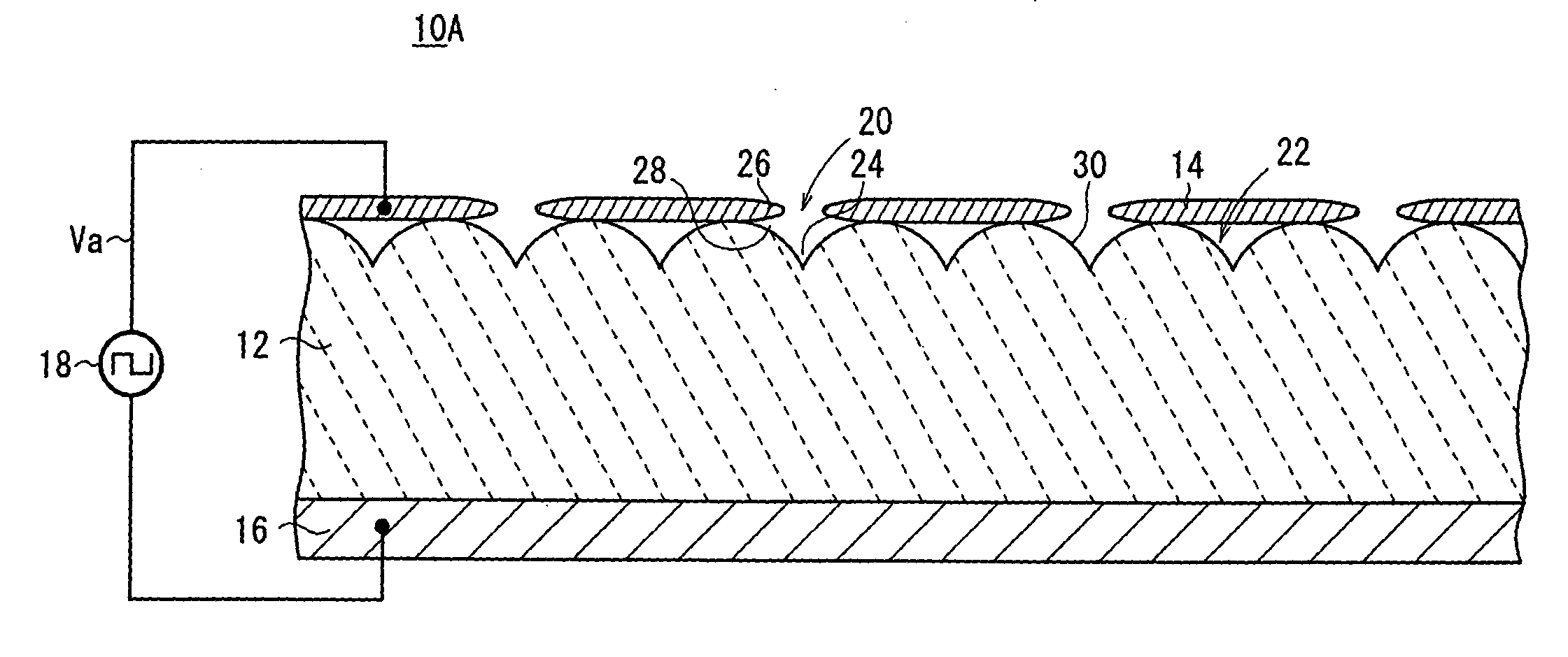
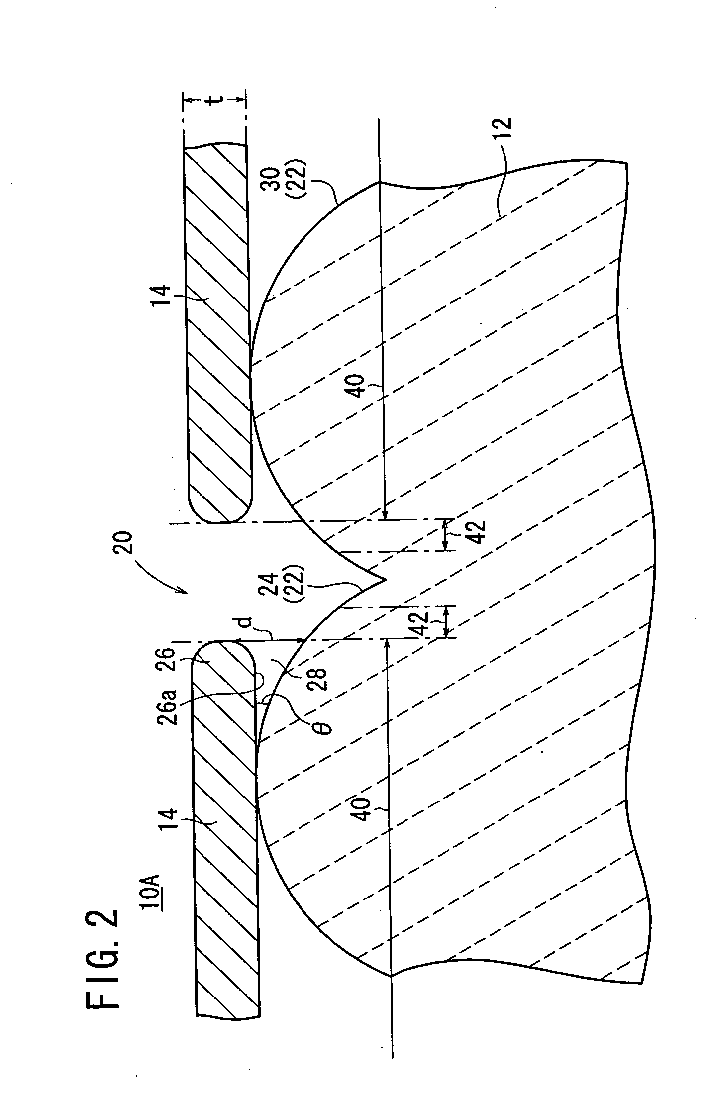
[0086] As shown in FIG. 1, an electron emitter 10A according to the present invention comprises a plate-like emitter 12 made of a dielectric material, a first electrode (e.g., an upper electrode) 14 formed on a first surface (e.g., an upper surface) of the emitter 12, a second electrode (e.g., a lower electrode) 16 formed on a second surface (e.g., a lower surface) of the emitter 12, and a pulse generation source 18 for applying a drive voltage Va between the upper electrode 14 and the lower electrode 16.
[0087] The upper electrode 14 has a plurality of through regions 20 where the emitter 12 is exposed. The emitter 12 has surface irregularities 22 due to the grain boundary of a dielectric material that the emitter 12 is made of. The through regions 20 of the upper electrode 14 are formed in areas corresponding to concavities 24 due to the grain boundary of the dielectric material. In the embodiment shown in FIG. 1, one through region 20 is formed in association with one concavity 24...
second embodiment
[0220] An electron emitter 10B according to the present invention will be described below with reference to FIG. 33.
[0221] As shown in FIG. 33, the electron emitter 10B according to the second embodiment has essentially the same structure as the electron emitter 10A according to the first embodiment described above, and resides in that the upper electrode 14 is made of the same material as the lower electrode 16, the upper electrode 14 has a thickness t greater than 10 μm, and the through region 20 is artificially formed by etching (wet etching or dry etching), lift-off, or a laser beam. The through region 20 may be shaped as the hole 32, the recess 44, or the slit 48, as with the electron emitter 10A according to the first embodiment described above.
[0222] The peripheral portion 26 of the upper electrode 14 has a lower surface 26a slanted gradually upwardly toward the center of the peripheral portion 26. The shape of the peripheral portion 26 can easily be formed by lift-off, for ...
third embodiment
[0227] An electron emitter 10C will be described below with reference to FIG. 37.
[0228] As shown in FIG. 37, the electron emitter 10C according to the third embodiment has essentially the same structure as the electron emitter 10A according to the first embodiment described above, but differs therefrom in that it has a single substrate 60 of ceramics, a lower electrode 16 formed on the substrate 60, an emitter 12 formed on the substrate 60 in covering relation to the lower electrode 16, and an upper electrode 16 formed on the emitter 12.
[0229] The substrate 60 has a cavity 62 defined therein at a position aligned with the emitter 12 to form a thinned portion to be described below. The cavity 62 communicates with the exterior through a through hole 64 having a small diameter which is defined in the other end of the substrate 60 remote from the emitter 12.
[0230] The portion of the substrate 60 below which the cavity 62 is defined is thinned (hereinafter referred to as “thinned port...
PUM
 Abstract
Description
Claims
Application Information