Method of growing GaN crystal, method of producing single crystal GaN substrate, and single crystal GaN substrate

a technology of gan crystal and sapphire, which is applied in the direction of crystal growth process, polycrystalline material growth, chemically reactive gas growth, etc., can solve the problems of poor symmetry depriving sapphire of cleavage plane, gan films or ingan films grown on sapphire substrates are annoyed by large lattice misfitting, and the sapphire has not been on the market. , to achieve the effect of eliminating hazy dislocation diffusion, large capacity

a technology of gan crystal and sapphire, which is applied in the direction of crystal growth process, polycrystalline material growth, chemically reactive gas growth, etc., can solve the problems of poor symmetry depriving sapphire of cleavage plane, gan films or ingan films grown on sapphire substrates are annoyed by large lattice misfitting, and the sapphire has not been on the market. , to achieve the effect of eliminating hazy dislocation diffusion, large capacity

US20050076830A1Inactive Publication Date: 2005-04-14SUMITOMO ELECTRIC IND LTD

Image

  • Method of growing GaN crystal, method of producing single crystal GaN substrate, and single crystal GaN substrate
  • Method of growing GaN crystal, method of producing single crystal GaN substrate, and single crystal GaN substrate
  • Method of growing GaN crystal, method of producing single crystal GaN substrate, and single crystal GaN substrate

Examples


embodiment 2 (

Observation Results)

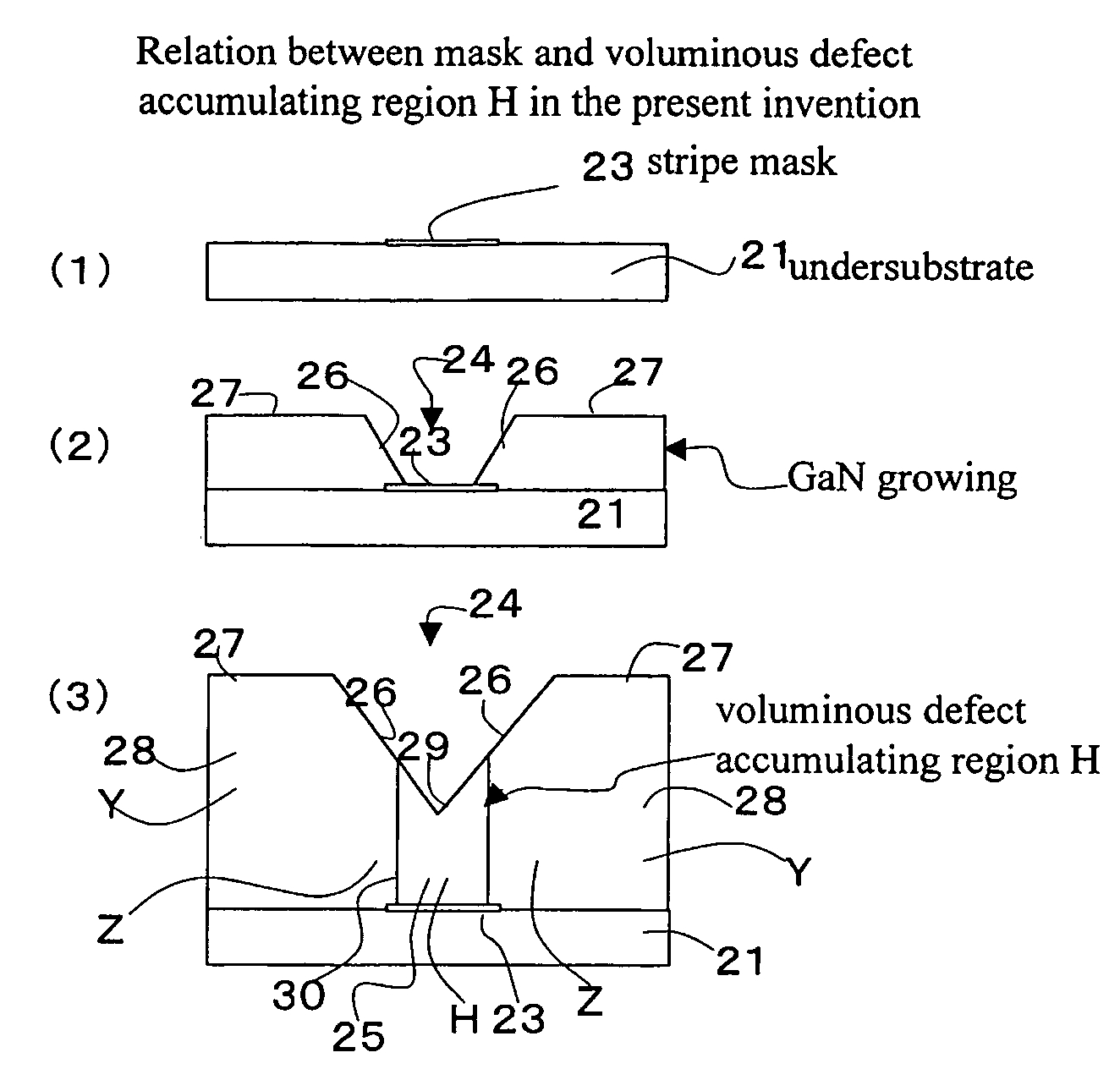
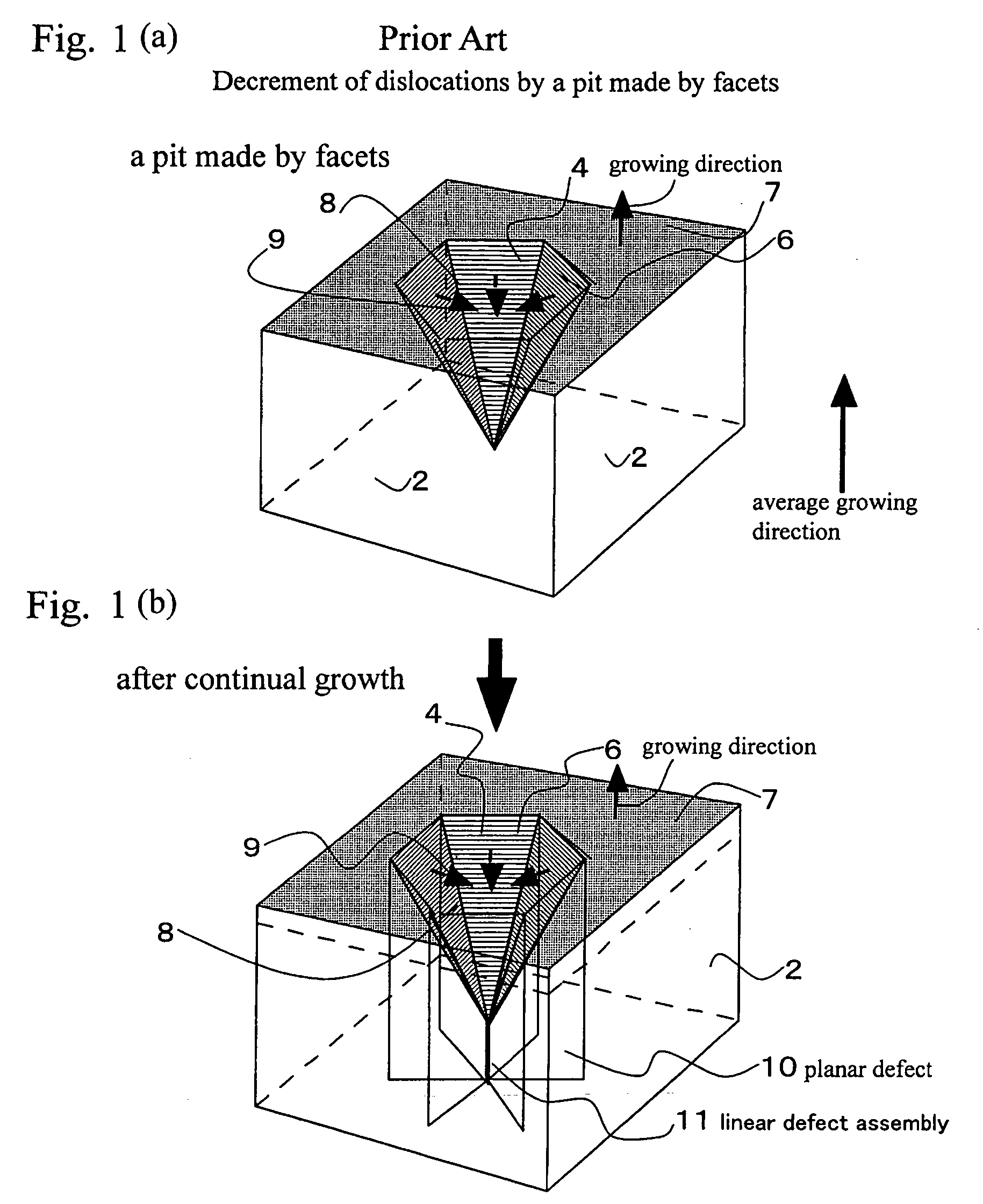
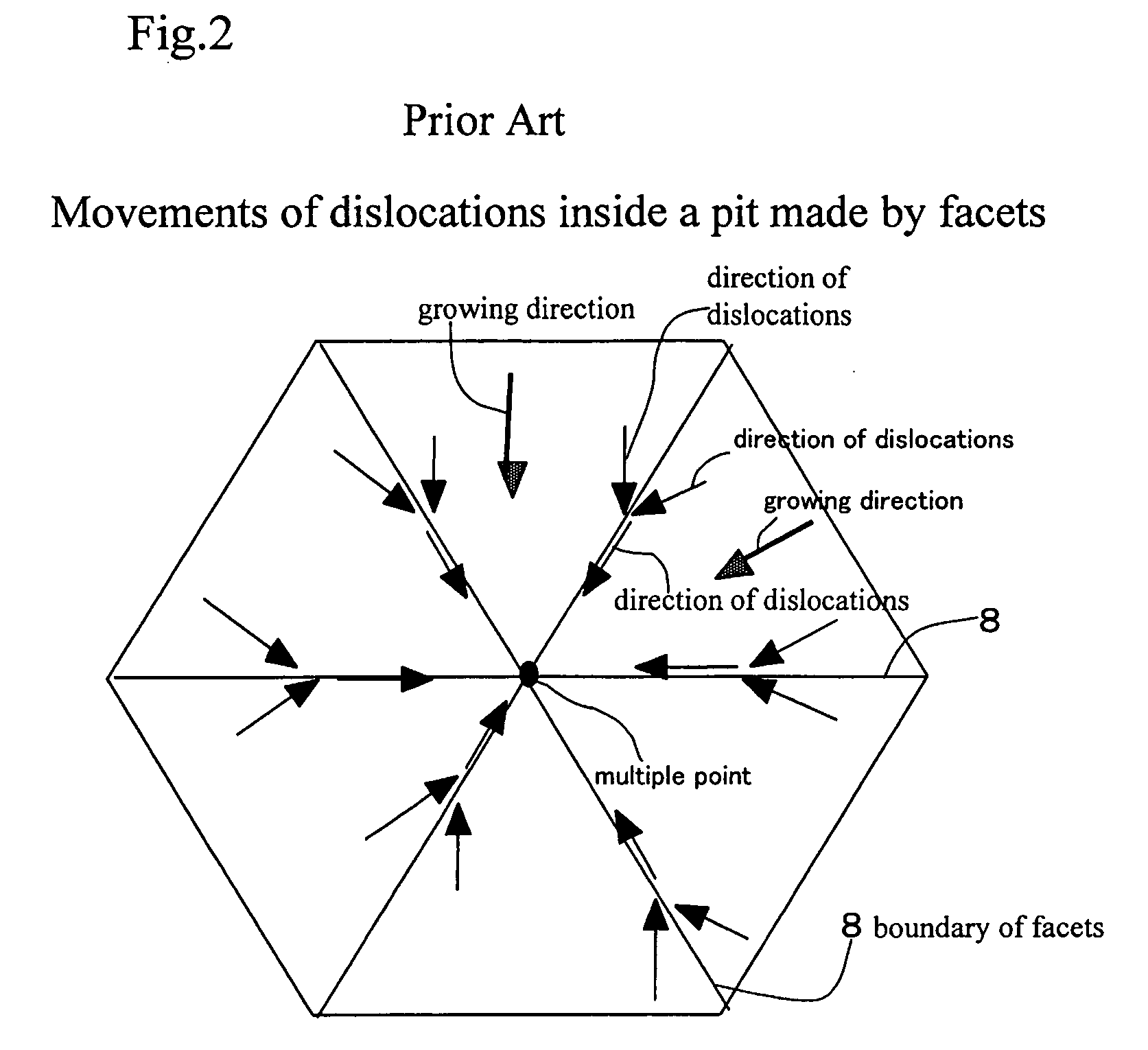
FIG. 9 shows a further contrived method of facet growth of GaN crystals. FIG. 9(1) denotes a part of a mask stripe 63 deposited upon an undersubstrate 61. The undersubstrate 61 is a single crystal wafer of GaAs (111). But, other materials, for example, Al2O3(sapphire), Si, SiC, MgO, ZnO, GaAs, InP, GaP, GaN, AlN are available for the undersubstrate. The parallel mask stripes 63 are formed on the undersubstrate 61 by evaporation, CVD, sputtering and photolithography. The stripe mask has a function of inhibiting epitaxial growth of GaN. GaN fine nuclei are grown in vapor phase by, e.g., HVPE on the masked undersubstrate at a low temperature below 700° C., for example, at 500° C.-650° C. Since a low temperature allows plenty of fine GaN nuclei to cover over the stripe mask 63 as well as non-masked parts 69 of the undersubstrate 61.

Then, GaN is grown in vapor phase at a high temperature more than 900° C., for example, at 1050° C. Such a high temperature prohibits G...


PUM

PropertyMeasurementUnit
temperatureaaaaaaaaaa

Abstract

A low dislocation density GaN single crystal substrate is made by forming a seed mask having parallel stripes regularly and periodically aligning on an undersubstrate, growing a GaN crystal on a facet-growth condition, forming repetitions of parallel facet hills and facet valleys rooted upon the mask stripes, maintaining the facet hills and facet valleys, producing voluminous defect accumulating regions (H) accompanying the valleys, yielding low dislocation single crystal regions (Z) following the facets, making C-plane growth regions (Y) following flat tops between the facets, gathering dislocations on the facets into the valleys by the action of the growing facets, reducing dislocations in the low dislocation single crystal regions (Z) and the C-plane growth regions (Y), and accumulating the dislocations in cores (S) or interfaces (K) of the voluminous defect accumulating regions (H).

Description

BACKGROUND OF THE INVENTION 1. Field of the Invention This invention relates to a method of producing a single crystal gallium nitride (GaN) substrate and a single crystal GaN substrate utilized as a substrate of making laser diodes (LDs) and light emitting diodes (LEDs) composed of groups 3-5 nitride semiconductors. 2. Description of Related Art Light emitting devices based upon group 3-5 nitride semiconductor include blue / green light emitting diodes and blue light laser diodes. Blue light LEDs have been sold on the market. But, LDs have not been on the market yet. Almost all of the conventional 3-5 nitride light emitting devices and laser diodes (LEDs, LDs) have been fabricated upon sapphire (α-Al2O3) substrates. Sapphire is a rigid and sturdy material. Sapphire excels in chemical and physical stability. Another advantage of sapphire is to allow GaN heteroepitaxial growth on it. Thus, GaN films, AlGaN films or InGaN films can be grown on sapphire substrates. Sapphire has been ...

Claims


Application Information

Patent Timeline
14 Apr 2005
Publication
US20050076830A1
IPC
C30B23/02; C30B25/02
CPC
C30B23/02; C30B29/406; C30B29/403; C30B25/02
Inventors
MOTOKI, KENSAKU; HIROTA, RYU