Image formation apparatus

a technology of image formation apparatus and spherical tube, which is applied in the direction of television systems, tubes with screens, instruments, etc., to achieve the effect of high display quality configuration

Inactive Publication Date: 2005-04-21
CANON KK
View PDF14 Cites 51 Cited by
  • Summary
  • Abstract
  • Description
  • Claims
  • Application Information

AI Technical Summary

Benefits of technology

[0008] It is an object of the present invention to provide an image formation apparatus capable of satisfying large-screen requirements and having a high display-quality configuration.

Problems solved by technology

However, the one using LCD is not of a self light-emitting type and has a problem of requiring a backlight, etc., and therefore a display apparatus of a self light-emitting type is needed.

Method used


Image

  • Image formation apparatus
  • Image formation apparatus
  • Image formation apparatus

Examples


examples 2 and 3

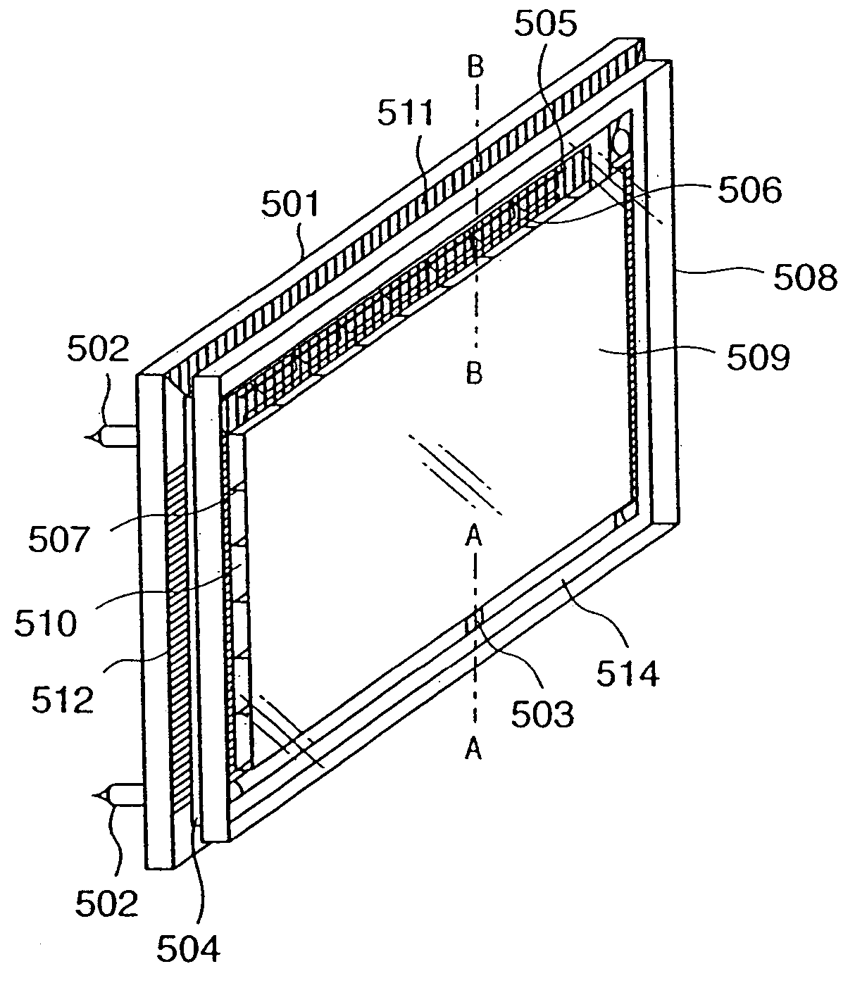
[0657] As Examples 2 and 3, an electron source with many plane type surface-conduction emission devices arranged in a simple matrix as shown in FIG. 18 was formed using printed wiring and combined with an image forming member to make up an image forming apparatus.

[0658] Referring to FIG. 89, the configuration and the production procedure of this example will be described below.

[0659] Examples 1 and 2 will be described.

[0660]FIGS. 89a to 89f are process drawings showing the production procedure of this example (here, a portion wired in matrix of 3×3, total 9, of devices situated at a corner of the image formation area as part of electron source on unillustrated substrate is shown). In FIGS. 89a to 89f, Numerals 212 and 213, denote a pair of device electrodes, 214 a conductive film for the formation of an electron emission part, 216 a first wiring layer, 217 a second layer and 218 an interlayer insulating film provided between the first wiring layer 216 and the second wiring layer ...

example 5

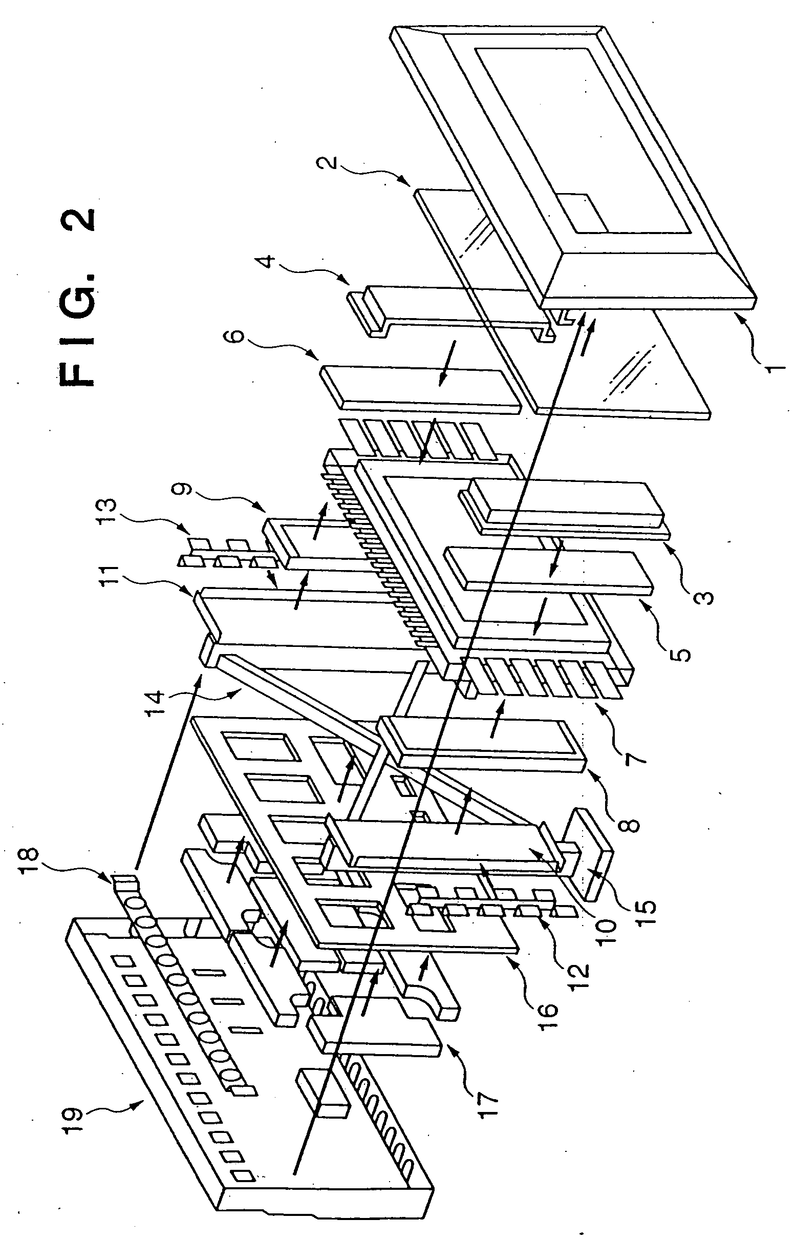
[0736] An image forming apparatus according to this example is fundamentally characterized in that the wiring is constructed by the screen print like FIGS. 97 and 101. One procedure of a method for manufacturing an image forming apparatus according to this example is shown in FIGS. 102a to 102d. Referring to FIG. 97, FIG. 100 and FIGS. 102a to 102d, a fundamental construction method and a manufacturing method of an image forming apparatus according to this example will be described below.

[0737] Step-a:

[0738] As with Example 1 of 17th Configuration, device electrodes 3202 and 3203 are formed on a cleaned glass substrate (FIG. 102a).

[0739] Step-b:

[0740] As with Example 1 of 17th Configuration, the wiring 3206 is formed. Here, a conductive member 3209 is simultaneously formed at a given position, i.e. at outer four corners of the image forming area (FIG. 102b). Incidentally, the distance between the conductive member 3209 and wires 3206 was set to approx. 200 μm or less.

[0741] Ste...

example 1

[1084] An image display apparatus of this example to which the 32nd configuration is applied will be described in reference with the FIG. 165. The FIG. 165 is a diagrammatically illustrated cross-section figure of the image display apparatus.

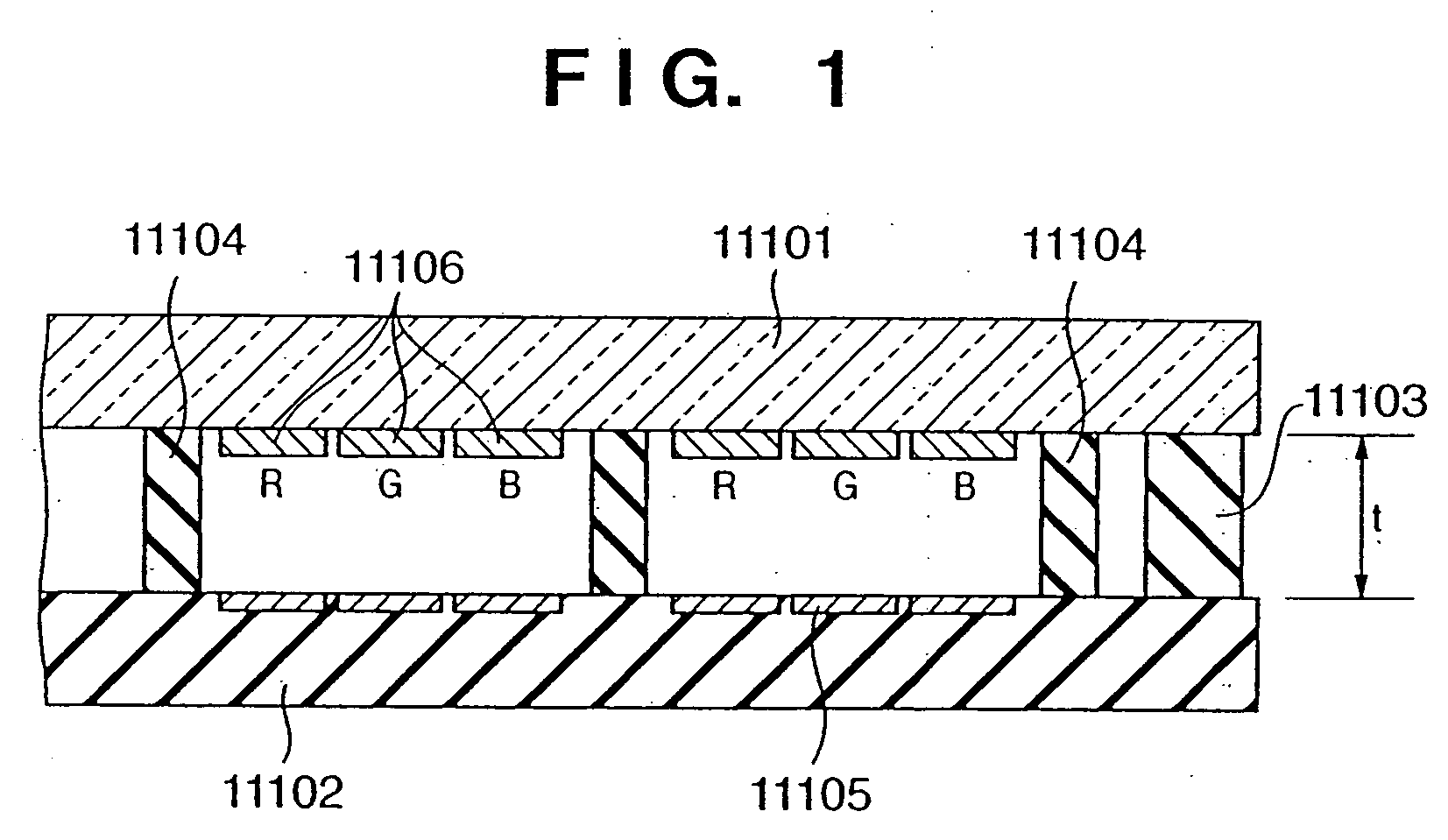
[1085] The image display apparatus is constituted by housing a display panel 4100 in an outer casing 4115. The display panel 4100 is constituted by installing a face plate 4107 on which fluorescent materials are arranged and a rear plate 4105 on which electron emission devices are arranged on the opposite to each other. The reference number 4101 denotes an air outlet for ventilating the warmed air in the panel to the outside by spontaneous convection and 4102 denotes an air inlet. The reference number 4103 is a front plate made of a transparent resin and installed as to protect and prevent the face plate 4107 from damages. The front plate 4103 may additionally be provided with a function of improving the contrast by inserting an optical filter....


PUM


Abstract

An image formation apparatus is disclosed which includes, within an enclosure configured by a pair of substrates placed face to face and an external frame placed between the substrates, an electron source placed on one of the pair of substrates, an image formation material placed on the other substrate, and spacers placed between the substrates, characterized in that the spacers and the external frame is conductive and device is provided for electrically connecting the spacers and the external frame so that the equipotential surfaces between the spacers and the external frame are quasi-parallel when driven.

Description

TECHNICAL FIELD [0001] The present invention relates to an image formation apparatus provided with an electron beam source substrate and a light-emitting display-plate placed face to face that forms an image by supplying electrons emitted from the electron beam source substrate according to image information to the light-emitting display plate. BACKGROUND ART [0002] Image display apparatuses equipped with an electron emission cathode of various configurations are conventionally proposed. As an example, the one having a structure whose cross-sectional view is shown in FIG. 1 is known. The display apparatus shown in FIG. 1 is a full-color display apparatus and has multiple stripe-shaped anode electrodes 11106 provided on the inner surface of an anode substrate 11101 and on the anode electrodes 11106 are formed surfaces on which fluorescent materials that emit R, G and B lights are sequentially deposited. On the other hand, on a cathode substrate 11102 facing the anode substrate 11101 ...

Claims


Application Information

Patent Timeline
Patent Type & Authority Applications(United States)
IPC IPC(8): G09G3/20G09G3/22G09G5/02H01J29/02H01J29/86H01J29/92H01J31/12H04N5/44H04N5/70H04N9/12H04N9/30
CPCG09G3/2011H04N9/30G09G3/22G09G5/02G09G2310/0229G09G2310/0267G09G2310/027G09G2320/0276G09G2320/0626G09G2330/02G09G2330/027G09G2330/04G09G2340/125H01J1/316H01J29/02H01J29/028H01J29/04H01J29/085H01J29/86H01J29/864H01J29/90H01J29/92H01J29/94H01J31/127H01J2201/3165H01J2201/319H01J2329/02H01J2329/0489H01J2329/323H01J2329/8625H01J2329/863H01J2329/864H01J2329/8645H01J2329/8655H01J2329/866H01J2329/90H01J2329/92H04N5/70H04N7/012H04N9/12G09G3/2014
Inventor MIYAZAKI, TOSHIHIKOONO, TAKEOMITSUTAKE, HIDEAKIHASEGAWA, MITSUTOSHIYAMAGUCHI, EIJIYAMADA, SHUJITODOKORO, YASUYUKI
Owner CANON KK
Why Eureka
Try Eureka