

Circuit board for large screen LED matrix array display
- Summary
- Abstract
- Description
- Claims
- Application Information
AI Technical Summary
Benefits of technology
Problems solved by technology
Method used
Image

Examples
second embodiment
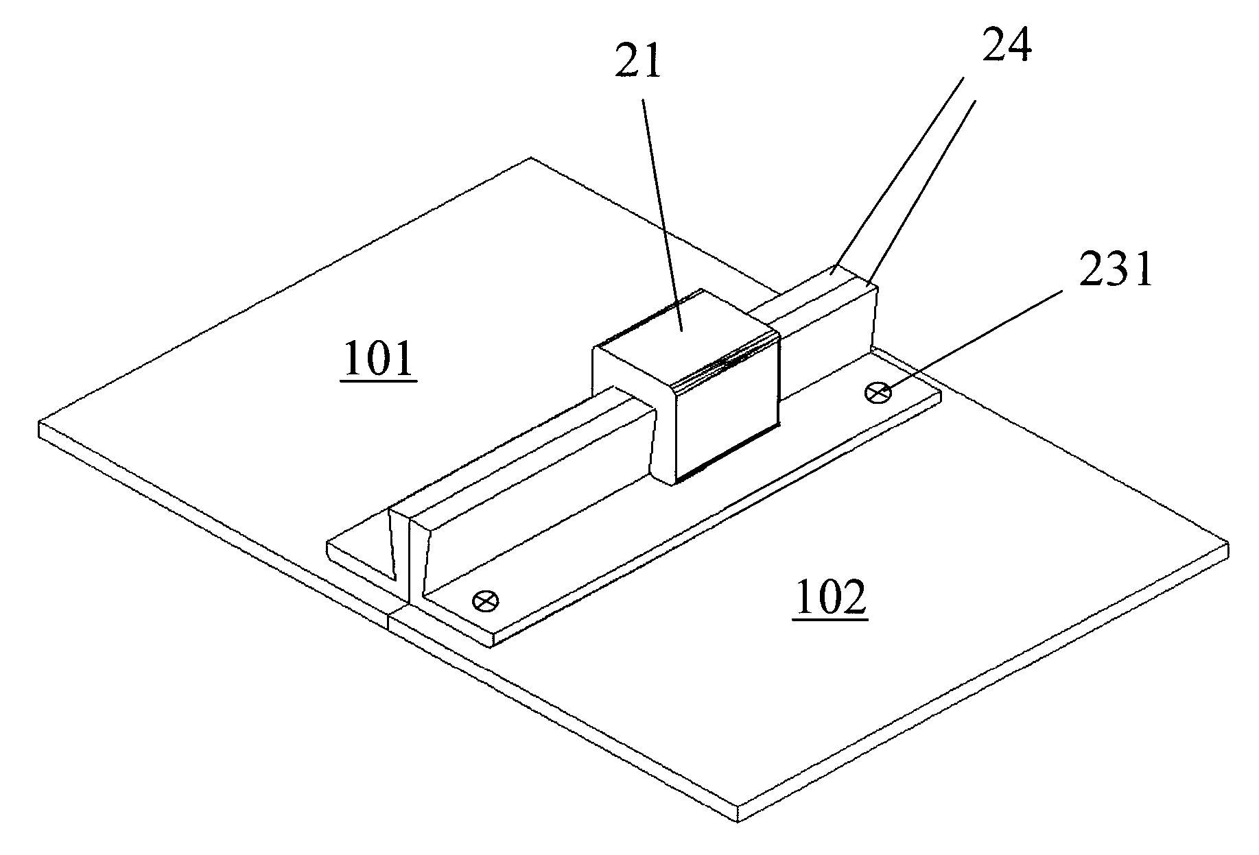
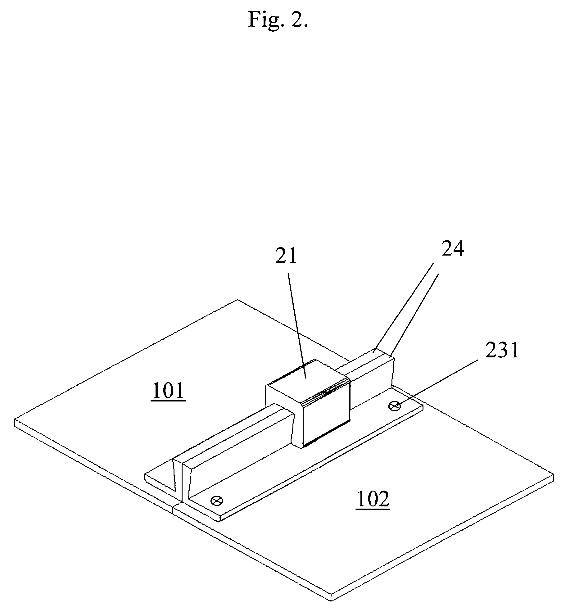
[0013]FIG. 3 shows the present invention. A set screw 23 is inserted on one jaw of the clamp 21. By tightening the set screw 23, the clamp can exert greater pressure to butt the two circuit boards 101, 102 together. Otherwise, the same reference numerals correspond to the same functional parts as in FIG. 2.
third embodiment
[0014]FIG. 4 shows the present invention. In addition to the horizontal set screw 23, an additional vertical set screw 233 is inserted on top of the clamp 21. The vertical set screw 233 exerts vertical pressure on the clamp, and prevents any misalignment of the two circuit boards 101, 102 in the vertical direction. Otherwise, the same reference numerals correspond to the same functional parts as in FIG. 2.
fourth embodiment
[0015]FIG. 5 shows the present invention A set screw 233 is inserted on top of the clamp 21 described in FIG. 2. The vertical set screw 233 exerts vertical pressure on the clamp 21, and presents any misalignment of the two circuit boards 101, 102 in the vertical direction. Otherwise, the same reference numerals correspond to the same functional part as in FIG. 2.
PUM
 Abstract
Description
Claims
Application Information