Light emitting display device

a display device and light-emitting technology, applied in the direction of static indicating devices, identification means, instruments, etc., can solve the problems of physical limit in increasing its density, deterioration of visual recognizability, and blemishes in resolution, so as to achieve the effect of limiting changes

Inactive Publication Date: 2005-04-21
TOHOKU PIONEER CORP
View PDF3 Cites 158 Cited by
  • Summary
  • Abstract
  • Description
  • Claims
  • Application Information

AI Technical Summary

Benefits of technology

[0020] The present invention relates to a display device in which a large number of above-described light emitting units are arranged in vertical and horizontal directions as described above to form a large display screen, and particularly, it is an object of the present invention to provide a display device which can be put into practical use by effectively restraining changes of the intensity characteristics which are due to the above-mentioned changes with time or changes in the light emission intensity accompanied by fluctuation of the environmental temperature and by being provided with a function by which the deterioration state of the display unit can be grasped.

Problems solved by technology

However, since each LED forms one dot (pixel) of an image, there is a physical limit in increasing its density, and there is a blemish in its resolution.
Thus, for example in a case where characters are displayed, visual recognizability is considerably deteriorated.
Thus, a result that the weight of an entire display device is increased is incurred.
Therefore, it is difficult to arrange continuing data electrode lines and scan electrode lines, covering the entire surface of a large display screen.
Even if this can be realized, in a case where utilizing ITO specifically as anode side data electrode lines is considered, the electrical resistance of the electrode lines becomes large, causing a difficulty in putting them to practical use, and further it becomes difficult to repair a defective part generated in a part of the screen.
However, in the case where respective light emitting display units by an EL display device are gathered to form a large area display screen as described above, technical problems to be solved as described below are supposed.
Such problems are problems of changes with time and temperature dependency of the intensity of an EL display element as described later and are problems of the practical lifetime of an EL display element, accompanied by changes with time of the intensity.
The organic EL element has a problem that variations in the initial intensity occur also due to for example variations in deposition at the time of film formation of this element, and thus it becomes difficult to express intensity gradation faithful to an input video signal.
A full color display device utilizing such a RGB method has a problem that color balance (white balance) drifts accompanied by passage of use time after all since cumulative light emission times of respective R, G and B elements differ and since respective speeds of the intensity decline differ due to light emission materials of respective organic EL elements constituting respective light emitting pixels of R, G and B.
Therefore, in a case where a full color display image by the parallel type RGB method is realized, there is a problem that color balance by respective R, G and B drifts similarly also by changes of the environmental temperature.
In the case where respective light emission display units by the EL display device are gathered to form a large area display screen as described above, following problems are expected to occur, being influenced by changes with time of intensities of EL display elements.
That is, for example in a case where some of light emitting display units are replaced in order to repair defective parts, an unnatural display condition in which only replaced parts are seen very brightly compared to other parts or the like is expected.
An organic EL element has a temperature dependency in the intensity thereof as described above although such a problem cannot necessarily be said to be a problem peculiar to the case where the light emitting display units are gathered.
Thus, the gathered units structure also has a technical problem that for example color balance drifts, being influenced by the environmental temperature.

Method used


Image

  • Light emitting display device
  • Light emitting display device
  • Light emitting display device

Examples


Embodiment Construction

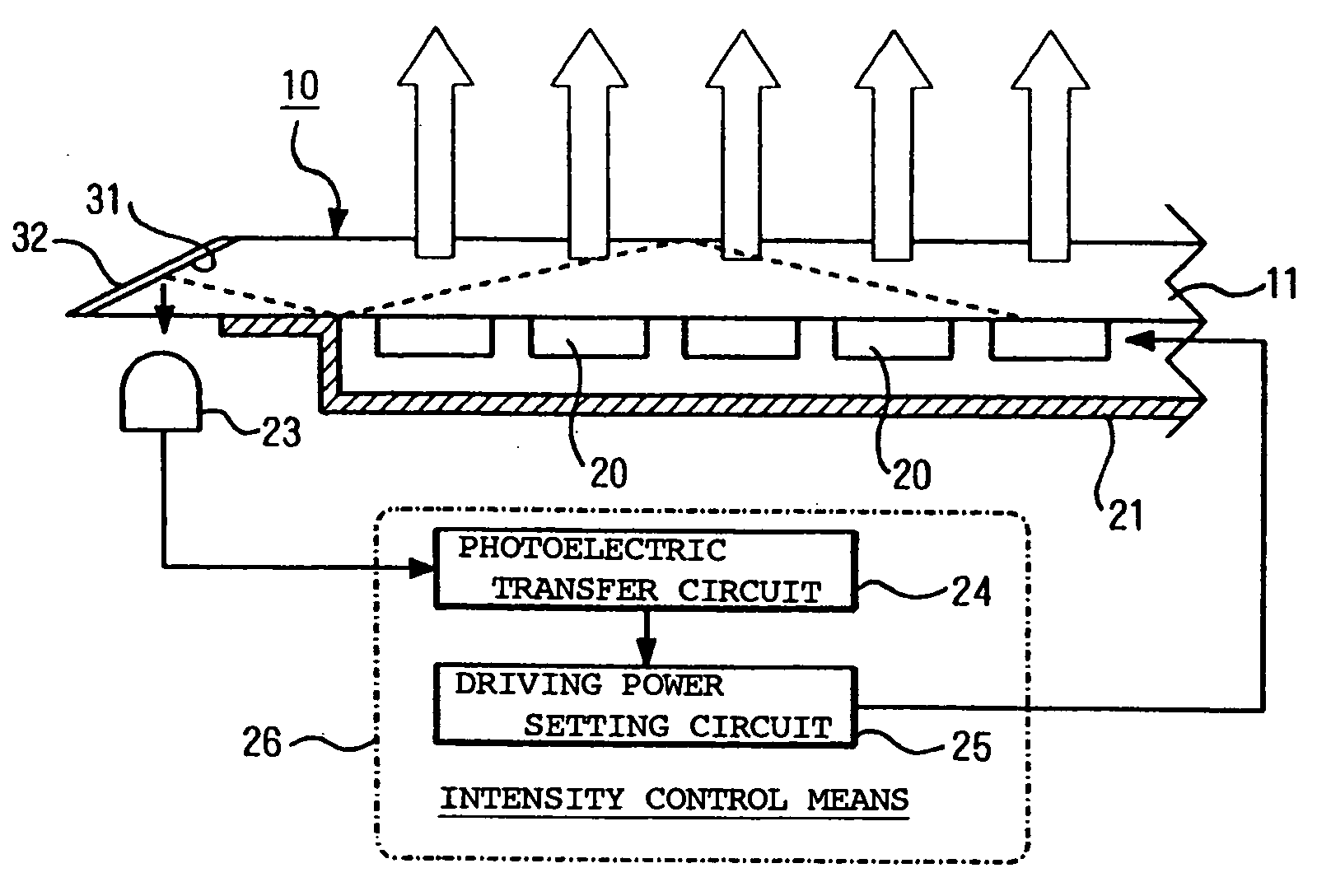
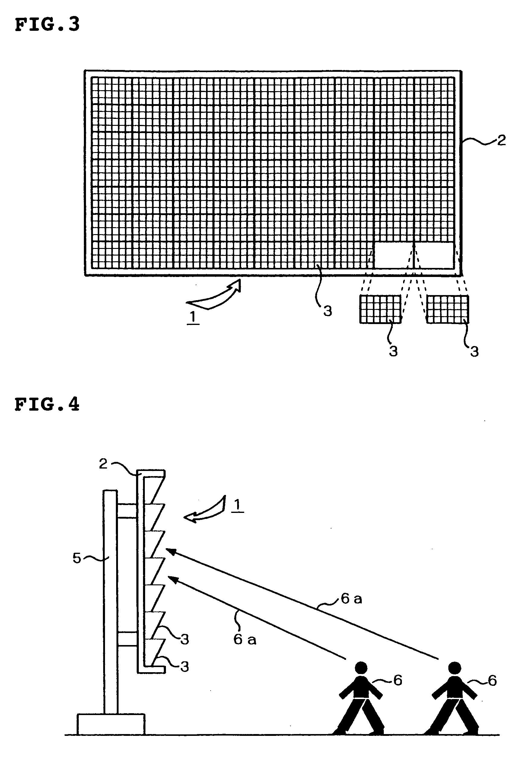
[0038] A light emitting display device according to the present invention will be described below with reference to the drawings. First, FIG. 3 schematically shows a state in which a display device according to the present invention is seen from the front thereof. As shown in FIG. 3, rectangular light emitting display units 3 in which organic EL elements are light emitting pixels are arranged in vertical and horizontal directions with respect to a rectangular frame body 2 constituting an outline of a light emitting display device 1 to form a light emitting display device by a large size screen. The respective light emitting display units 3, as depicted in a lower right part of FIG. 3, are detachably constructed with respect to the rectangular frame body 2, and with this structure, maintenance work such as replacement for the light emitting display unit 3 or the like can be implemented as the need arises.

[0039] The respective light emitting display units 3 hold drive ICs or the like...


PUM


Abstract

A light emitting display device 1 characterized by forming one display screen by combining a plurality of light emitting display units comprising intensity control means for measuring a light emission intensity by a light emitting element (organic EL element 20) which is formed above/on a transparent substrate 11 and which includes an anode electrode 12, a cathode electrode 16, at least one organic light emission functional layer (13,14,15) between the electrodes to control the light emission intensity of the light emitting element above/on the substrate 11 within a predetermined range and deterioration state reporting means for detecting a deterioration state of the light emitting element above/on the substrate 11 to report the state.

Description

BACKGROUND OF THE INVENTION [0001] 1. Field of the Invention [0002] The present invention relates to a light emitting display device in which a light emitting display panel provided with an intensity control function that can set the light emission intensities of light emitting elements to a predetermined value respectively and individually and a deterioration state reporting function that can detect and report a deterioration state of a light emitting element is employed and which forms a large size display screen by arranging a large number of these light emitting display panels. [0003] 2. Description of the Related Art [0004] For example in an event place or hall, a theater, a sports ground, or the like, in order to provide video information for a large number of audiences / spectators, a display device equipped with a large area display screen is installed. In recent years, also in monitoring operation circumstances of various plants and the like, monitoring traffic information, o...

Claims


Application Information

Patent Timeline
Patent Type & Authority Applications(United States)
IPC IPC(8): H05B33/12G09F9/00G09F9/30G09F9/40G09G3/20G09G3/30G09G5/00H01L27/32H01L51/50H05B33/14
CPCG09G3/3216G09G3/3233G09G2360/145G09G2320/041G09G2320/043G09G2300/026H05B45/60Y02B20/30
Inventor SUZUKI, GENYAZAWA, NAOKI
Owner TOHOKU PIONEER CORP
Why Eureka
Try Eureka