Eureka AIR delivers breakthrough ideas for toughest innovation challenges, trusted by R&D personnel around the world.

Semiconductor light emitting device, backlight, color image display device and phosphor to be used for them

a technology of semiconductors and light emitting devices, which is applied in the direction of luminescence, lighting and heating apparatus, instruments, etc., to achieve the effects of high durability, excellent luminance and emission efficiency, and broad color reproducibility

Active Publication Date: 2013-07-23
CITIZEN ELECTRONICS CO LTD +1
View PDF41 Cites 85 Cited by
  • Summary
  • Abstract
  • Description
  • Claims
  • Application Information

AI Technical Summary

Benefits of technology

[0059]According to the present invention, it is possible to obtain a light emitting device capable of accomplishing broad color reproducibility by a light emitting device comprising a light emitting device to emit light with a specific wavelength and phosphors having specific characteristics in combination, and it is further possible to obtain a light emitting device which is excellent in luminance and emission efficiency and has high durability. Further, by using such a light emitting device as a light source and properly prescribing the relation between the NTSC ratio and the light use efficiency, it is possible to realize reproduction of deep red and green without impairing brightness of the image thereby to accomplish broad color reproducibility as the entire image. Further, red, green and blue emissions can be carried out by one chip, whereby it is possible to provide a color image display device without impairing the productivity in its mounting and whereby adjustment of the white balance is easy.

Problems solved by technology

Inversely, if the brightness is increased, the NTSC ratio tends to be low, and it tends to be difficult to reproduce a vivid image.
However, in the above light source, the yellow emitting phosphor was used, whereby emission with wavelengths unnecessary from the viewpoint of the color purity of red and green was substantial, and it was difficult to obtain a display with high color reproducibility (High Gamut).
Here, it is possible, at least in principle, to increase the color purity of red and green by cutting off light with unnecessary wavelengths by means of a color filter, but as mentioned above, if it is attempted to increase the NTSC ratio by adjusting the color filter in order to reproduce the vivid color image, the majority of emission of the backlight will be cut off, whereby there has been a problem that the brightness decreases substantially.
Especially, by this method, emission of red decreases substantially, whereby it has been practically impossible to reproduce a strongly reddish color.
However, in such a color image display device, LED chips independent for red, green and blue, respectively, are combined, whereby there have been problems such that 1) it takes time and labor to mount them, 2) since the respective LED chips for red, green and blue are disposed at finite distances, it is required to take the distance of an optical waveguide to be long to sufficiently mix emitted lights from the respective LED chips, and 3) since the white chromaticity is adjusted by combining the integral multiple of the respective LED chips, adjustment of the white balance can not be continuously carried out.
However, in a case where such semiconductor light emitting devices are practically combined with color filters to constitute color image display devices for e.g. liquid crystal displays, there have been cases where the emission of backlight tends to be inadequate, or chromaticity deviation is likely to occur.
However, with respect to the demand for high performance in recent years, the specifically disclosed light emitting device employing the 3.5MgO.0.5MgF2.GeO2:Mn4+ type, Y2O3:Eu type and YVO4:Eu3+ type phosphors, is inadequate from the viewpoint of the emission efficiency, etc., and it is desired to develop one having higher performance.
However, by a study by the present inventors, it has been found that such a light emitting device undergoes substantial deterioration of the properties and is not practically durable for a reason assumed to be such that hydrogen fluoride is generated by the reaction with moisture in air, and it has been desired to develop one having a higher performance.
Further, with a view to suppressing deterioration of phosphors, it is known to cover the surface of water-soluble phosphor particles with a coating of e.g. a metal oxide (Patent Document 8), but such a method requires a special apparatus and is inadequate from the viewpoint of the types of the useful phosphors, etc.Non-Patent Document 1: Monthly display, April 2003 issue (p 42-46)Patent Document 1: WO2005 / 111707Patent Document 2: JP-A-2002-171000Patent Document 3: U.S. Pat. No. 6,809,781Patent Document 4: WO2004 / 025359Patent Document 5: U.S. Patent Application Publication No. 2006 / 0071589Patent Document 6: U.S. Patent Application Publication No.

Method used


Image

  • Semiconductor light emitting device, backlight, color image display device and phosphor to be used for them
  • Semiconductor light emitting device, backlight, color image display device and phosphor to be used for them
  • Semiconductor light emitting device, backlight, color image display device and phosphor to be used for them

Examples


embodiment (

(3-4-3) Embodiment (c)

[0473]With respect to a light emitting device having the above-mentioned structure (c), one embodiment is shown in FIG. 24 to describe it specifically.

[0474]In FIG. 24, the circumference of a material layer B (111) which is a fluoride complex phosphor-containing layer, is covered by a material layer E (114) which is a layer of a material not containing a fluoride complex phosphor.

[0475]The material to constitute the material layer E is particularly preferably one not having groups reactive with the fluoride complex phosphor, and it may, for example, be a fluorinated saturated or unsaturated hydrocarbon resin or a silicone resin.

[0476]The weight average molecular weight of the resin to constitute the material layer E as measured by a GPC method may, for example, be the same one as the molecular weight of the resin to constitute the above-mentioned material layers C and D.

[0477]Further, the thickness of the above material layer D may depend also on the size of th...

preparation example 1

(1-1) Preparation Example 1

Red Emitting Phosphor K2Tif6:Mn (Hereinafter Sometimes Referred to Also as “KTF”)

[0645]So that the feedstock composition for a phosphor would be K2 Ti0.95 Mn0.05 F6, as raw material compounds, K2 TiF6 (4.743 g) and K2 MnF6 (0.2596 g) were slowly added and dissolved in 40 ml of hydrofluoric acid (47.3 wt %) with stirring under atmospheric pressure at room temperature. After the respective raw material compounds were all dissolved, 60 ml of acetone was added at a rate of 240 ml / hr while stirring the solution to let a phosphor precipitate in the poor solvent. The obtained phosphor was washed with pure water and acetone, respectively, followed by drying at 100° C. for one hour. The obtained phosphor was confirmed to be K2 TiF6:Mn by X-ray diffraction pattern.

preparation example i-2

(1-2) Preparation Example I-2

Green Emitting Phosphor Ba3Si6O12N2:Eu (Hereinafter Sometimes Referred to as “BSON”)

[0646]So that the feedstock composition for a phosphor would be Ba2.7Eu0.3Si6.9O12N3.2, as raw material compounds, BaCO3 (267 g), SiO2 (136 g) and Eu2O3 (26.5 g) were thoroughly stirred and mixed, and then filled in an alumina crucible. This mortar was placed in a resistance heating type electric furnace equipped with a temperature adjuster, heated to 1,100° C. at a temperature raising rate of 5° C. / min under atmospheric pressure, held at that temperature for 5 hours and then left to cool to room temperature. The obtained sample was pulverized to at most 100 μmm in the alumina crucible.

[0647]The obtained sample (295 g) and Si3N4 (45 g) as a raw material compound were thoroughly stirred and mixed, and then filled in an alumina mortar for primary firing, and this crucible was heated to 1,200° C. under atmospheric pressure while circulating a gas mixture of 96 vol % of nitro...


PUM

PropertyMeasurementUnit
specific surface areaaaaaaaaaaa
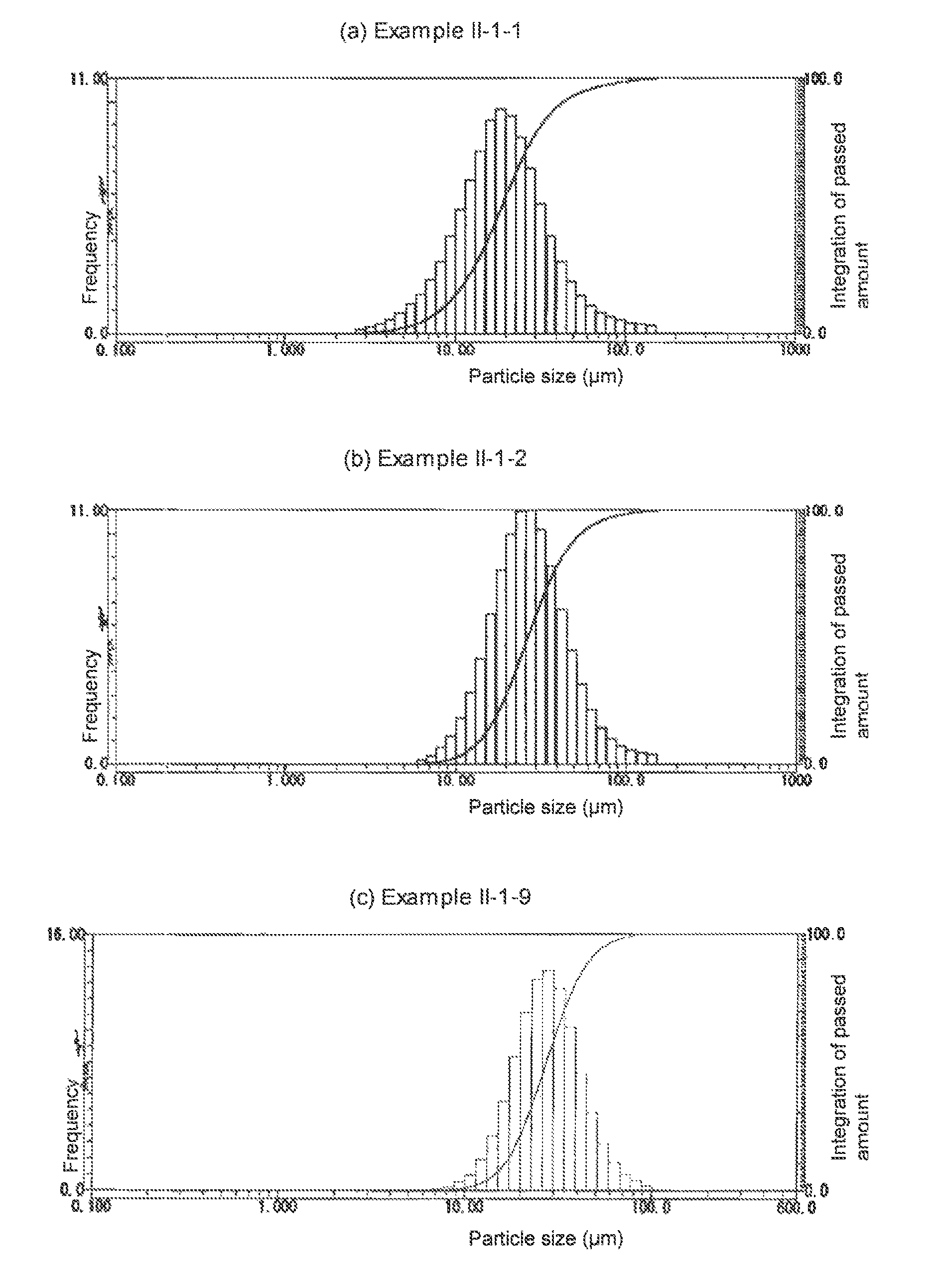
weight-average median diameter D50aaaaaaaaaa

Abstract

To provide a semiconductor light emitting device which is capable of accomplishing a broad color reproducibility for an entire image without losing brightness of the entire image.A light source provided on a backlight for a color image display device has a semiconductor light emitting device comprising a solid light emitting device to emit light in a blue or deep blue region or in an ultraviolet region and phosphors, in combination. The phosphors comprise a green emitting phosphor and a red emitting phosphor. The green emitting phosphor and the red emitting phosphor are ones, of which the rate of change of the emission peak intensity at 100° C. to the emission intensity at 25° C., when the wavelength of the excitation light is 400 nm or 455 nm, is at most 40%.

Description

TECHNICAL FIELD[0001]The present invention relates to a semiconductor light emitting device useful for a color image display device to realize an image with a high color purity, and a backlight employing it. Further, the present invention relates to a color image display device to realize an image with a high color purity to meet with the emission wavelength of an improved backlight, a novel phosphor suitable for such a semiconductor light emitting device and a process for its production.BACKGROUND ART[0002]In recent years, liquid crystal display devices are used not only in the conventional application to personal computer monitors but also in application to ordinary color televisions. The color reproduction range of the color liquid crystal display devices is determined by colors of light emitted from the red, green and blue pixels and, where chromaticity points of the respective color pixels in the CIE XYZ colorimetric system are represented by (xR,yR), (xG,yG) and (xB,yB), the c...

Claims


Application Information

Patent Timeline
Patent Type & Authority Patents(United States)
IPC IPC(8): C09K11/08H01L33/50
CPCC09K11/616G02F1/1336H01L33/504F21K2/00H05B33/14G02B6/0023H01L2224/45144G02B6/0038G02B6/0043G02B6/0053G02F1/133603G02F1/133609G02F1/133611G02F1/133615G02F2001/133614G02F2001/133624H01L2224/48091H01L2224/48247H01L2924/3025H01L2224/45124H01L24/45H01L2224/45015H01L2924/00014H01L2924/20752H01L2924/20753H01L2924/00H01L2924/12042H01L2924/12044H01L2924/12041H01L2924/181F21V3/062C09K11/0883C09K11/675C09K11/7734C09K11/7739G02F1/133614G02F1/133624C09K11/77347C09K11/77342C09K11/77348H01L2924/00012G02F1/133602H01L33/50H01L33/52F21Y2115/10G02B6/0073G02F1/133514G02F1/133528G02F1/1368H01L33/502
Inventor HONG, BYUNGCHULSAKO, NAOKIKIJIMA, NAOTOYOSHINO, MASAHIKOHASE, TAKASHIYOYASU, FUMIKOHORIBE, KENTAROU
Owner CITIZEN ELECTRONICS CO LTD
Why Eureka
Eureka Blog
Learn More