Organic electroluminescent display device of top emission type

a display device and electroluminescent technology, applied in the direction of static indicating devices, identification means, instruments, etc., can solve the problem of limiting the array pattern of emissive regions, and achieve the effect of influencing (variance in luminance or life cycle)

Inactive Publication Date: 2005-04-28
SANYO ELECTRIC CO LTD
View PDF2 Cites 49 Cited by
  • Summary
  • Abstract
  • Description
  • Claims
  • Application Information

AI Technical Summary

Benefits of technology

[0031] Furthermore, the emissive regions respectively corresponding to each of the colors can be formed having an area of different from each other. Therefore, influence (variance in luminance or life cycle) ca

Problems solved by technology

This causes limitation on the arra

Method used


Image

  • Organic electroluminescent display device of top emission type
  • Organic electroluminescent display device of top emission type
  • Organic electroluminescent display device of top emission type

Examples


first embodiment

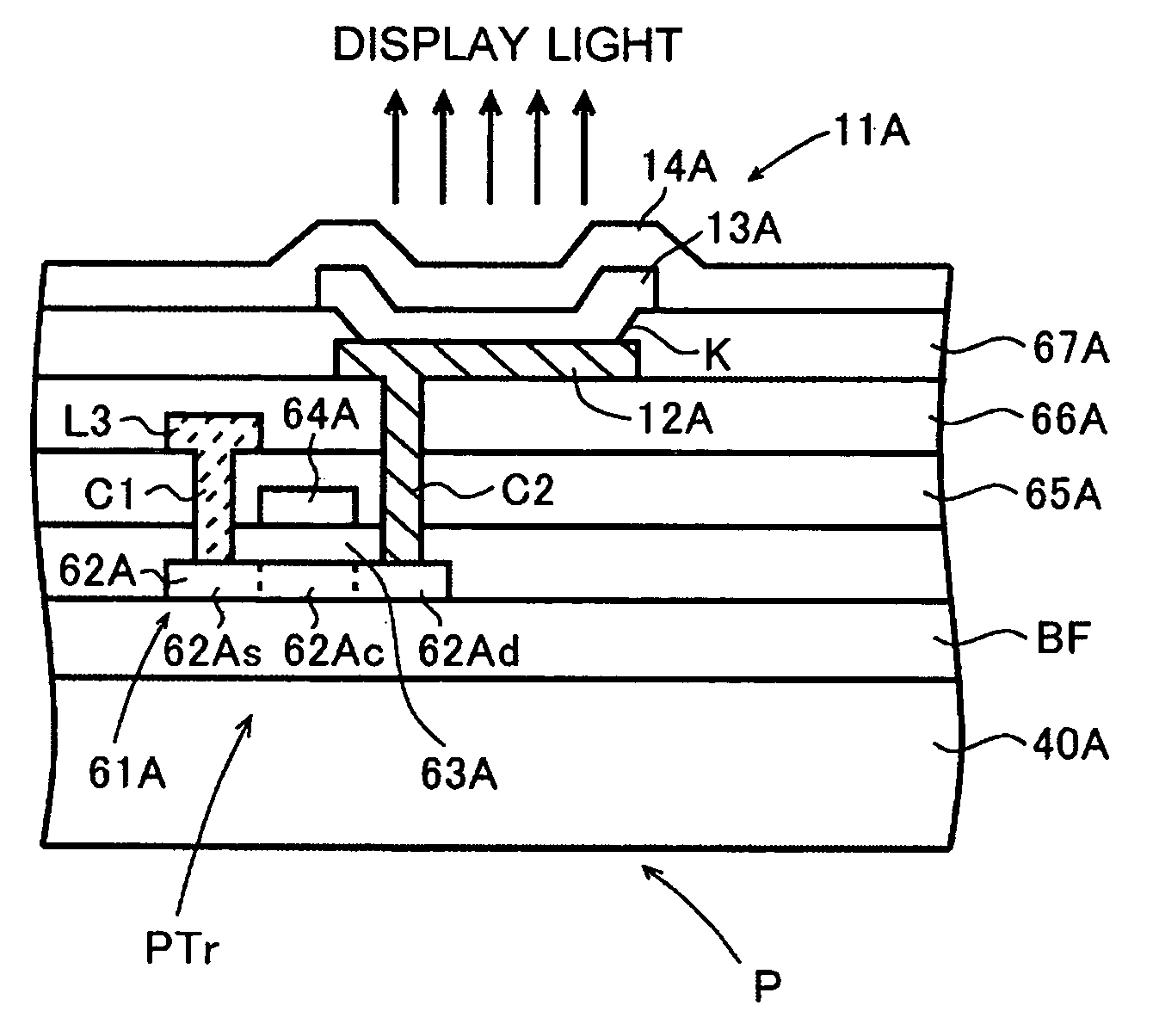
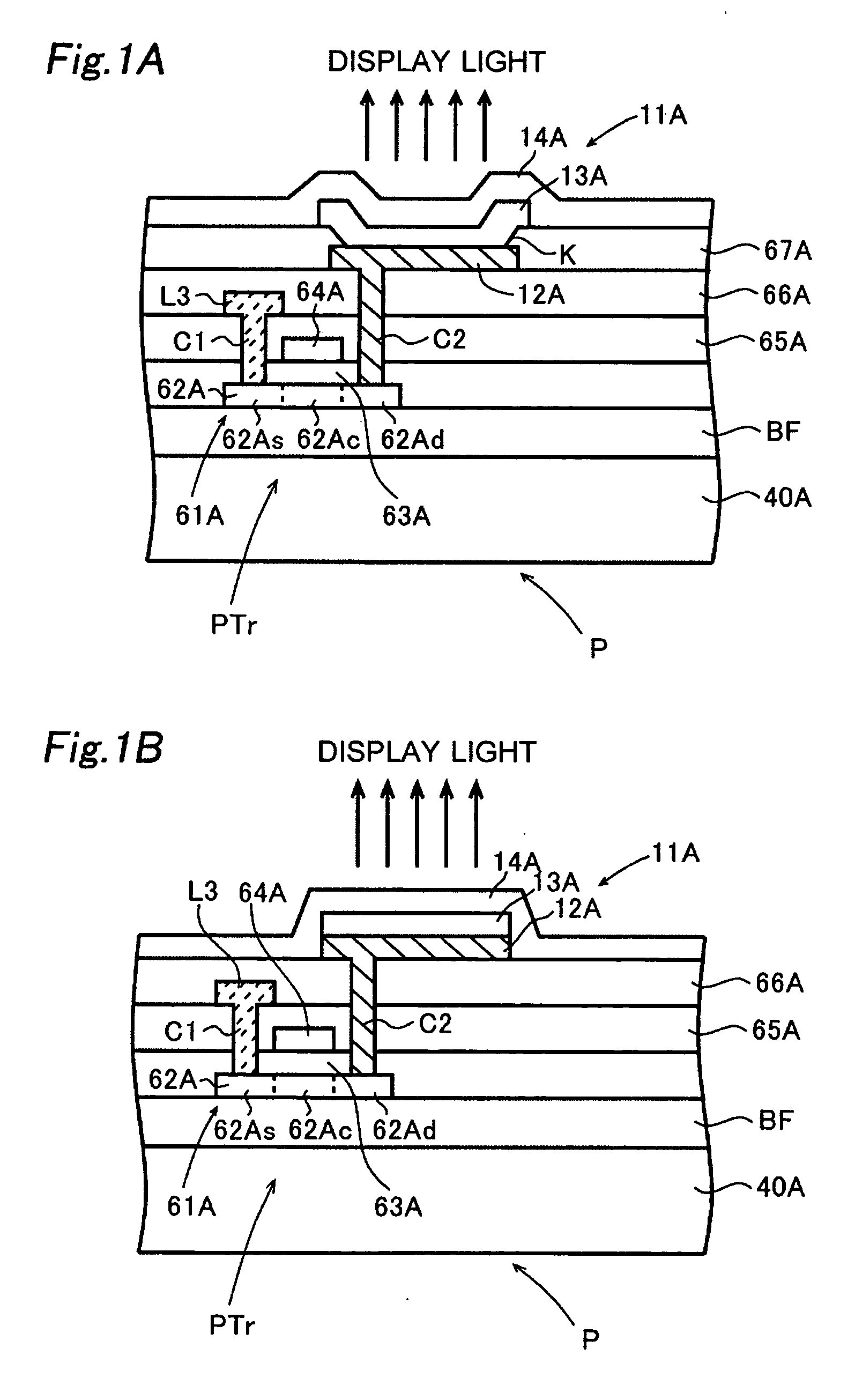
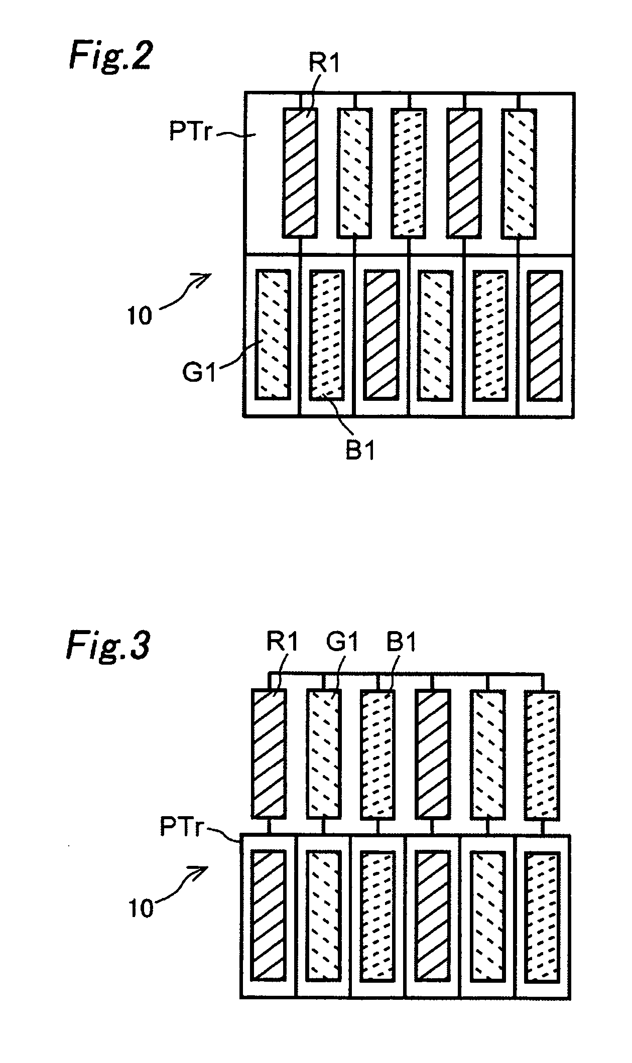
[0063]FIG. 2 is a plan view showing a display portion 10 of the organic EL display device of top emission type of the invention. A plurality of TFT formation regions PTr of the pixels P, that is, a plurality of regions where the driving TFT 61A, the pixel selecting TFT 71A, and the storage capacitor Cs are formed, is formed in a rectangular shape and disposed in a stripe array on the display portion 10. Emissive regions R1, G1 and B1 of the organic EL element 11A respectively forming each of the pixels P are formed in a rectangular shape with same size, and placed in a delta array over the adjacent TFT formation regions PTr.

second embodiment

[0064]FIG. 3 is a plan view showing a display portion 10 of an organic EL display device of top emission type of a A plurality of TFT formation regions PTr is formed in a rectangular shape and disposed in a delta array on the display portion 10. Emissive regions R1, G1, and B1 are respectively formed in a rectangular shape with the same size and disposed in a stripe array, lying over the adjacent TFT formation regions PTr in the alternate rows where the TFT formation regions PTr are shifted.

third embodiment

[0065]FIG. 4 is a plan view showing a display portion 10 of an organic EL display device of top emission type of a A plurality of TFT formation regions PTr is formed in a rectangular shape and disposed in a stripe array on the display portion 10. Emissive regions R1, G1 and B1 respectively form a rectangular shape having size different from each other, and are placed in a stripe array over the adjacent TFT formation regions PTr (for example, extending in a first (row) direction over the pixels P arrayed in a matrix).


PUM


Abstract

In an organic EL display device, emissive regions are arrayed in various patterns without depending on array patterns of the TFT formation regions and so on. A plurality of TFT formation regions PTr of pixels P is formed in a stripe array on a display portion. Emissive regions R1 of the organic EL element 11A emitting red light, emissive regions G1 of the organic EL element 11A emitting green light, and emissive regions B1 of the organic EL element 11A emitting blue light are arrayed on these TFT formation regions PTr. The emissive regions R1, G1, and B1 are disposed in delta array over the adjacent TFT formation regions PTr.

Description

CROSS-REFERENCE OF THE INVENTION [0001] This invention is based on Japanese Patent Application No. 2003-330929, the content of which is incorporated by reference in its entirety. BACKGROUND OF THE INVENTION [0002] 1. Field of the Invention [0003] This invention relates to an organic electroluminescent display device, particularly to an organic electroluminescent display device where flexibility in array positions of emissive regions of organic electroluminescent elements is increased [0004] 2. Description of the Related Art [0005] In recent years, organic electroluminescent (hereafter, referred to as EL) display devices using EL elements are receiving attention as a new display device substituted for a CRT or an LCD. Particularly, an organic EL display device having thin film transistors (hereafter, referred to as TFTS) as switching elements for driving the organic EL elements is being developed. [0006] A bottom emission type and a top emission type have been known in the organic EL...

Claims


Application Information

Patent Timeline
IPC IPC(8): G09F9/30H05B33/12G09G3/30H01L27/32H01L29/04H01L51/50H05B33/00H05B33/14
CPCH01L27/3211H01L2251/5315H01L27/3244G09G2300/0452G09G3/3208H10K59/352H10K59/353H10K59/12H10K2102/3026H05B33/00H05B33/12
Inventor MATSUMOTO, SHOICHIRONISHIKAWA, RYUJI
Owner SANYO ELECTRIC CO LTD
Why Eureka
Try Eureka