Ultra-shallow junction MOSFET having a high-k gate dielectric and in-situ doped selective epitaxy source/drain extensions and a method of making same

a technology of epitaxy source/drain extension and ultra-shallow junction, which is applied in the direction of basic electric elements, electrical apparatus, semiconductor devices, etc., can solve the problems of gate oxide damage, gate-electrode-to-source extension bridging, damage, etc., and achieve the effect of reducing or ameliorating leakage currents

Active Publication Date: 2005-05-05
TAIWAN SEMICON MFG CO LTD
View PDF8 Cites 65 Cited by
  • Summary
  • Abstract
  • Description
  • Claims
  • Application Information

AI Technical Summary

Benefits of technology

[0007] The present invention contemplates a semiconductor device, such as a MOSFET, preferably a USJ MOSFET, having a high-k gate dielectric, a source and a drain, and extensions thereof formed by in-situ doped selective epitaxy techniques. Preferably, the source and the drain are deep, while the extensions are shallow. The present invention also contemplates a method of fabricating such a MOSFET which eliminates or ameliorates leakage currents between the gate electrode and the source / drain extensions caused by pre-epitaxy and / or epitaxy procedures.
[0009] In accordance with another preferred embodiment of the present invention, a MOSFET is provided. The MOSFET comprises a semiconductor substrate and a gate on a free surface of the substrate. The gate includes a gate dielectric, which comprises a layer of high-k material on the free surface of the substrate, and a gate electrode on the free surface of the high-k layer. The high-k layer protrudes beyond the gate electrode and is capable of acting as a protective barrier against damage during etching, cleaning, HF dip, epitaxial procedures, or epitaxial-related procedures. The MOSFET also comprises a source and a drain formed on opposite sides of the gate, and a shallow source extension and a shallow drain extension formed by selective in-situ doped epitaxy.

Problems solved by technology

Following fabrication of the above-described smaller, faster MOSFETs using epitaxial techniques to form the source and drain and having a thin gate oxide, damage to the gate oxide has been detected.
Such damage causes gate-electrode-to-source-extension bridging or gate-electrode-to-drain-extension bridging.
It is postulated that such damage is caused by the processes typically effected prior to and during the epitaxial steps carried out to produce the source, the drain and their extensions.
Such damage gives rise to excessive gate leakage current and device failure following formation of the selective epitaxy source and drain and / or their extensions.

Method used


Image

  • Ultra-shallow junction MOSFET having a high-k gate dielectric and in-situ doped selective epitaxy source/drain extensions and a method of making same
  • Ultra-shallow junction MOSFET having a high-k gate dielectric and in-situ doped selective epitaxy source/drain extensions and a method of making same
  • Ultra-shallow junction MOSFET having a high-k gate dielectric and in-situ doped selective epitaxy source/drain extensions and a method of making same

Examples


Embodiment Construction

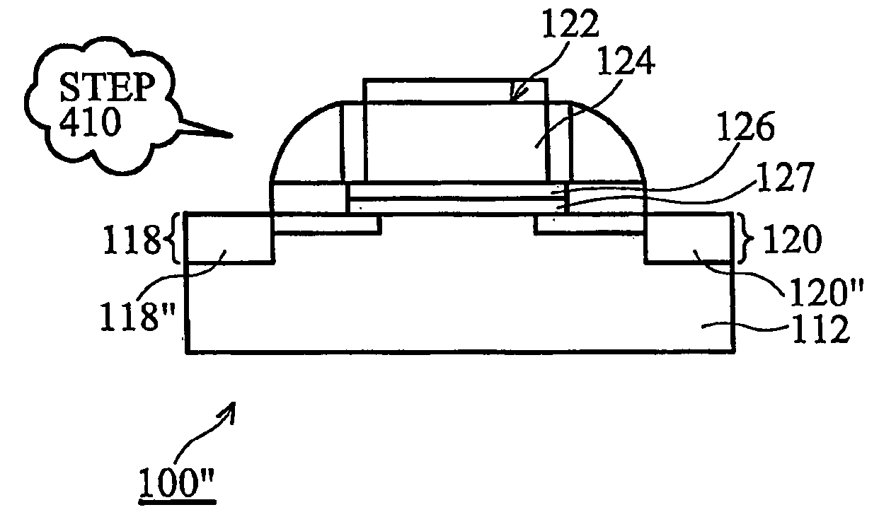
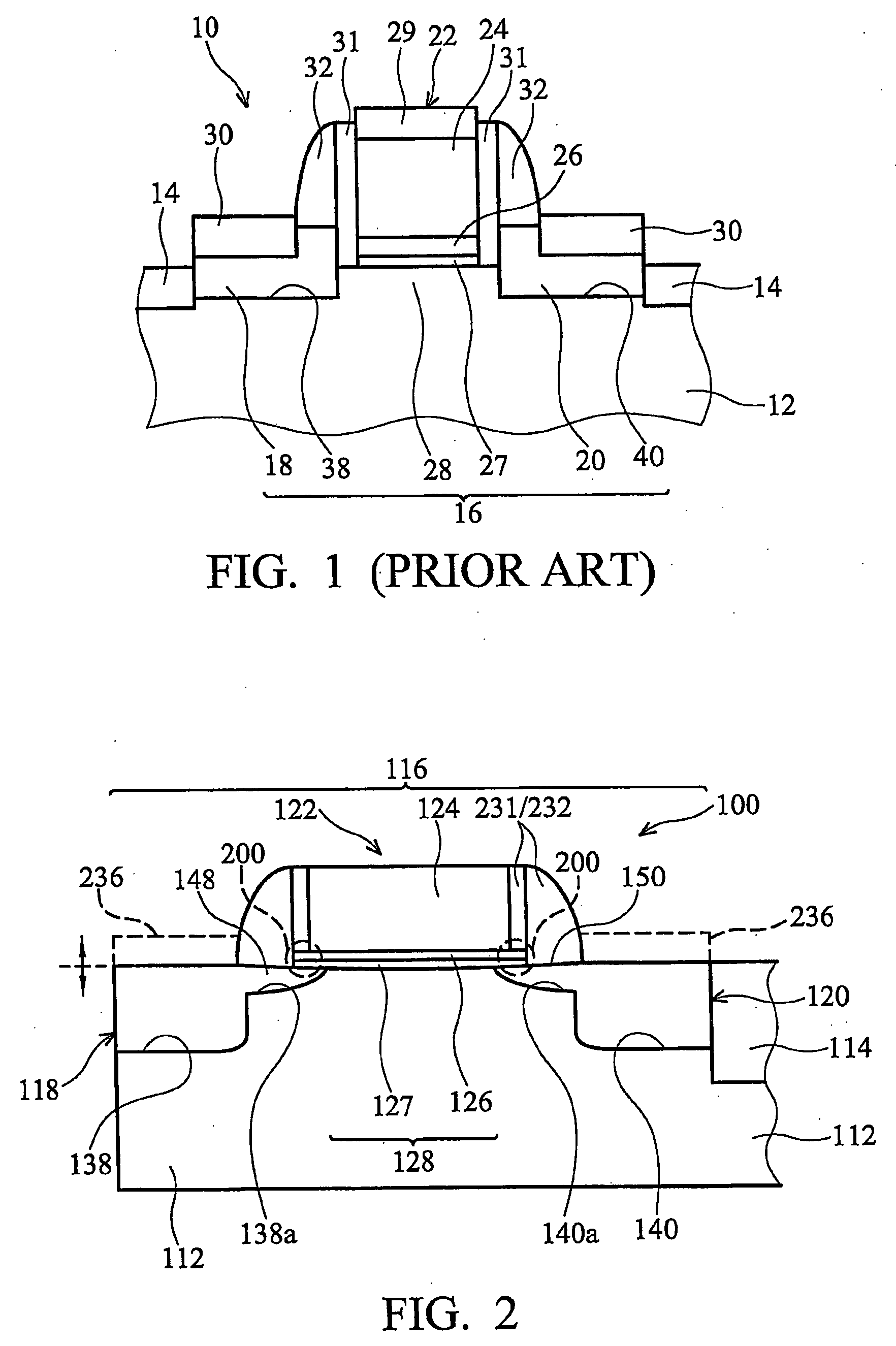
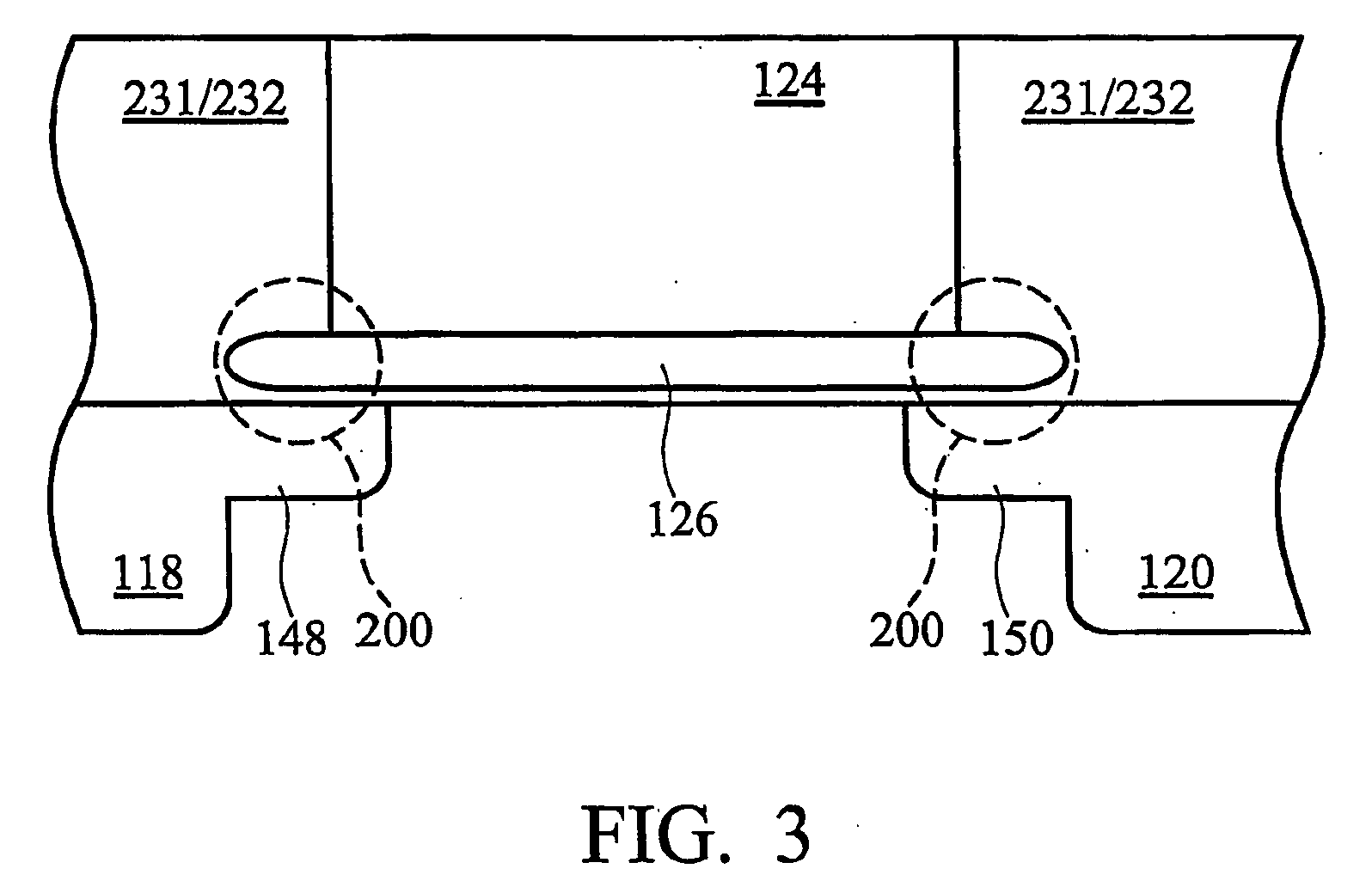
[0019] The making and using of the presently preferred embodiments are discussed in detail below. It should be appreciated, however, that the present invention provides many applicable inventive concepts that can be embodied in a wide variety of specific contexts. The specific embodiments discussed are merely illustrative of specific ways to make and use the invention, and do not limit the scope of the invention.

[0020] In its product embodiments, a MOSFET has a semiconductor substrate, such substrate including both a semiconductor layer on an insulative substrate (“SOI”) and a semiconductor body (“bulk”). The term “MOSFET” will be understood by those skilled in the art to include single or multiple transistors, memory cells, and other semiconductor devices, as well as both NMOS and PMOS devices. The substrate may comprise any suitable semiconductor including (typically) silicon, silicon-germanium, silicon-carbon and germanium.

[0021] An active region of the substrate is defined bet...


PUM


Abstract

A MOSFET includes a gate having a high-k gate dielectric on a substrate and a gate electrode on the gate dielectric. The gate dielectric protrudes beyond the gate electrode. A deep source and drain having shallow extensions are formed on either side of the gate. The deep source and drain are formed by selective in-situ doped epitaxy or by ion implantation and the extensions are formed by selective, in-situ doped epitaxy. The extensions lie beneath the gate in contact with the gate dielectric. The material of the gate dielectric and the amount of its protrusion beyond the gate electrode are selected so that epitaxial procedures and related procedures do not cause bridging between the gate electrode and the source / drain extensions. Methods of fabricating the MOSFET are described.

Description

[0001] This application claims priority to provisional patent application Ser. No. 60 / 516,500, filed Oct. 31, 2003, and entitled “Ultra-Shallow Junction MOSFET Having a High-k Gate Dielectric and In-Situ Doped Selective Epitaxy Source / Drain Extensions and a Method of Making Same,” which application is incorporated herein by reference.TECHNICAL FIELD [0002] The present invention relates to ultra shallow junction (“USJ”) MOSFETs having high-k gate dielectrics and in-situ doped selective epitaxy source / drain extensions. The present invention also relates to methods of fabricating such MOSFETs. More specifically, the present invention relates to MOSFETs of the foregoing description which exhibit improved performance relative to prior art MOSFETs, and to methods by which such MOSFETs may be fabricated. BACKGROUND [0003] Prior art MOSFETs include a source and a drain formed in an active region of a semiconductor layer (semiconductor-on-insulator or “SOI” format) or of a semiconductor body...

Claims


Application Information

Patent Timeline
Patent Type & Authority Applications(United States)
IPC IPC(8): H01L21/28H01L21/336H01L29/10H01L29/51H01L29/78
CPCH01L21/28194H01L29/1054H01L29/513H01L29/517H01L29/7833H01L29/6653H01L29/6656H01L29/66636H01L29/518
Inventor WANG, CHIH-HAOCHEN, SHANG-CHIHWANG, YEN-PINGCHIU, HSIEN-KUANGYAO, LIANG-GIHU, CHENMING
Owner TAIWAN SEMICON MFG CO LTD
Why Eureka
Try Eureka