Plasma display panel and method of manufacturing back panel thereof

a technology of display panel and back panel, which is applied in the manufacture of electric discharge tubes/lamps, gas exhaustion means, instruments, etc., can solve the problems of prone to cracking, rough surface of back plate, and increased risk of damage to back pla

Inactive Publication Date: 2005-05-05
SAMSUNG SDI CO LTD
View PDF15 Cites 13 Cited by
  • Summary
  • Abstract
  • Description
  • Claims
  • Application Information

AI Technical Summary

Benefits of technology

[0016] The present invention provides a Plasma Display Panel (PDP), which includes a back plate having a structure that prevents cracking around a ventilation hole and damage to a periphery of the ventilation hole caused by a jig used to move the back plate, and a method of manufacturing the back panel of the plasma display panel.

Problems solved by technology

Thus, when the operation of forming the hole in the back plate is completed, the back plate becomes more vulnerable to damage.
Specifically, the surface ofthe back plate becomes rough, and the area around the ventilation hole is prone to cracking.
This increases manufacturing overhead of the back plate.
However, when the ventilation hole is not distanced from the cut by more than a predetermined threshold length, the area around the ventilation hole is even more prone to cracking, and the back plate can be damaged.
Specifically, since an end portion of the back plate is coupled to a jig during manufacture and handling, stress is applied to the crack, and the back plate can be damaged more.

Method used


Image

  • Plasma display panel and method of manufacturing back panel thereof
  • Plasma display panel and method of manufacturing back panel thereof
  • Plasma display panel and method of manufacturing back panel thereof

Examples


first embodiment

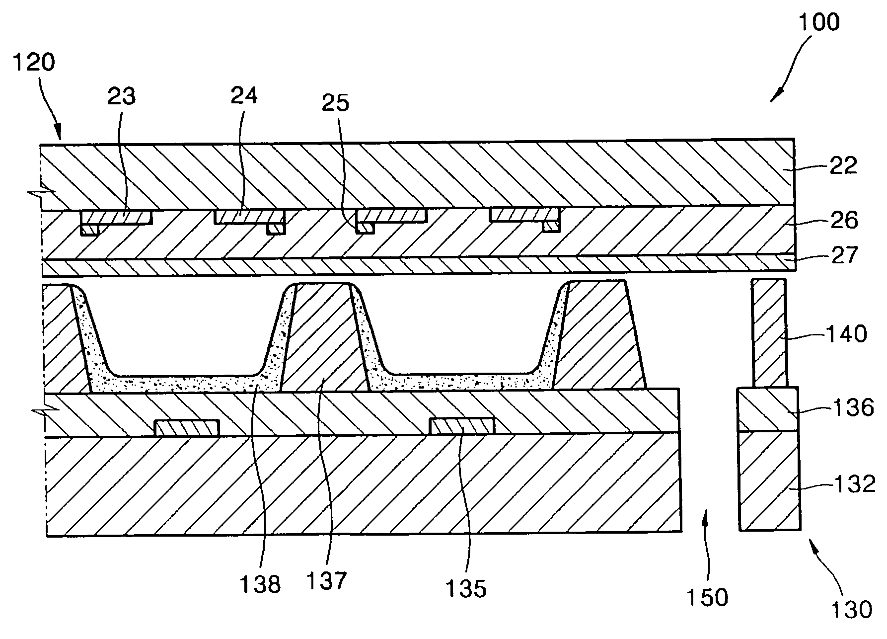
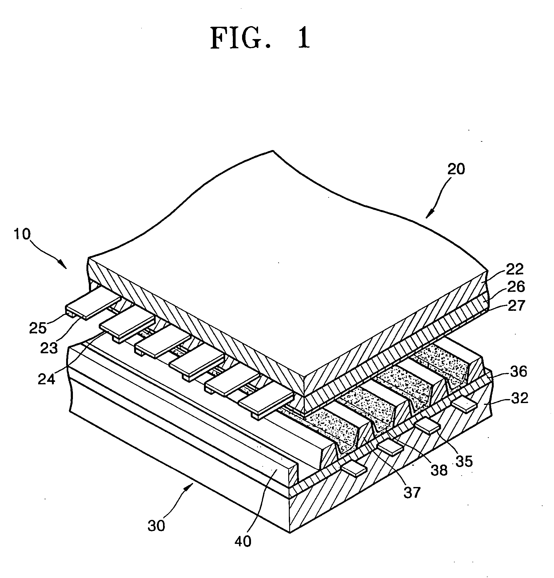
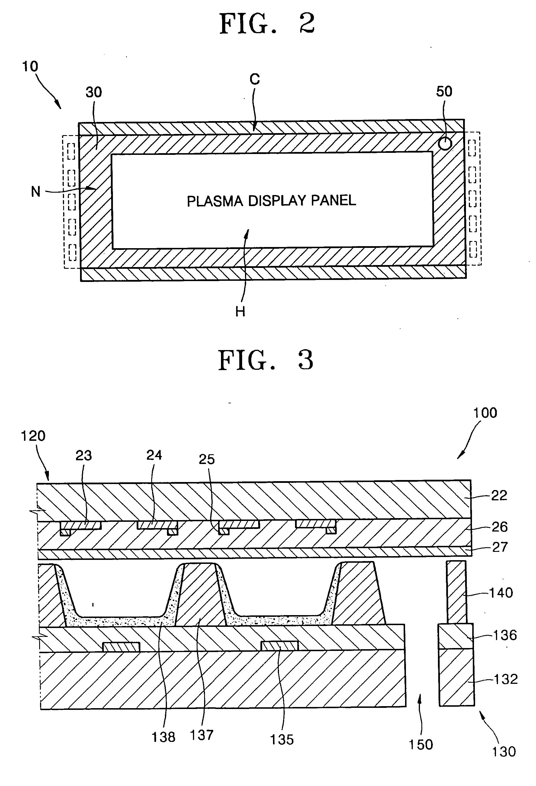
[0053] Referring to FIG. 3, a Plasma Display Panel (PDP) 100 according to the present invention includes a front panel 120 and a back panel 130 facing the front panel 120. In FIG. 3, the front panel 120 is rotated at an angle of 90°. A front plate 22 is arranged on the front panel 120. A plurality of electrodes including X electrodes 23, Y electrodes 24, and bus electrodes 25 are arranged on the front plate 22.

[0054] The plurality of electrodes 23, 24, and 25 are arranged in predetermined patterns, for example, a stripe pattern or a zigzag pattern. If the PDP 100 according to the first embodiment of the present invention is an AC PDP, a front dielectric layer 26 can be arranged on the front plate 22 and a protective layer 27 is arranged on the front dielectric layer 26, as shown in FIG. 3. The back panel 130 facing the front panel 120 includes a back plate 132, a plurality of electrodes 135, and at least one ventilation hole 150. Furthermore, a barrier rib 137 and a phosphor layer 1...

second embodiment

[0065]FIG. 7 is a view of a PDP 200 according to the present invention. In FIG. 7, a front plate 22 is rotated by 90° for convenience.

[0066] Referring to FIG. 7, the PDP 200 according to the second embodiment of the present invention includes a front panel 220 having the front plate 22 and a plurality of electrodes 23, 24, and 25 arranged on a surface of the front plate 22 in a predetermined pattern. The PDP 200 also includes a back panel 230 having a back plate 232 facing the front plate 22, a plurality of electrodes 235 arranged on a surface of the back plate 232 corresponding to the electrodes of the front plate 22 and arranged in a predetermined pattern, and a ventilation hole 250.

[0067] The ventilation hole 250 is formed after forming the plurality of electrodes 235, a back dielectric layer 236, a barrier rib 237, and a phosphor layer 238 on a surface of the back plate 232. In addition, the front panel 220, on which the front plate 22 and the electrodes 23, 24, and 25 are arra...


PUM


Abstract

A Plasma Display Panel (PDP) includes: a front panel having a front plate and a plurality of electrodes arranged on a surface of the front plate in a predetermined pattern and a back panel having a back plate facing the front plate, a plurality of electrodes arranged on a surface of the back plate in a predetermined pattern to correspond to the plurality of electrodes of the front plate, and at least one ventilation hole. At least two back plates are formed by cutting one base plate on which at least two ventilation holes are formed. Each ventilation hole has a first width in a first edge direction of the back plate and a distance from the first edge to a center of the at least one ventilation hole is at least twice that of the first width.

Description

CLAIM OF PRIORITY [0001] This application makes reference to, incorporates the same herein, and claims all benefits accruing under 35 U.S.C. §119 from an application for PLASMA DISPLAYPANEL COMPRISING A BACK PANEL AND MANUFACTURING METHOD OF THE BACK PANEL OF PLASMA DISPLAY PANEL earlier filed in the Korean Intellectual Property Office on 9 Oct. 2003 and there duly assigned Serial No. 2003-70284. BACKGROUND OF THE INVENTION [0002] 1. Field of the Invention [0003] The present invention relates to a Plasma Display Panel (PDP) and a method of manufacturing a back panel of the PDP, and more particularly, to a PDP that forms an image by applying a discharge voltage to a plurality of electrodes arranged on two substrates facing each other to generate ultraviolet rays which excite phosphor layers and a method of manufacturing the back panel. [0004] 2. Description of the Related Art [0005] Plasma display panels (PDPs) can be classified into Direct Current (DC) PDPs and Alternating Current (...

Claims


Application Information

Patent Timeline
Patent Type & Authority Applications(United States)
IPC IPC(8): H01J9/24H01J9/385H01J11/12H01J11/20H01J11/24H01J11/26H01J11/34H01J17/16
CPCH01J9/241H01J11/54H01J11/12H01J9/385H01J11/34
Inventor HONG, CHONG-GIKANG, TAE-KYOUNG
Owner SAMSUNG SDI CO LTD
Why Eureka
Try Eureka