Light emitting device, driving method of light emitting device and electronic device

a technology of light emitting device and electronic device, which is applied in the direction of static indicating device, electroluminescent light source, instruments, etc., can solve the problems of easy dispersion of characteristics, short life of oled due to organic luminescent layer deterioration, and inability to compare the electric characteristics of tft utilizing polysilicon, etc., to prevent the luminance of light emitting element from dispersing, constant luminance, and prevent the effect of light emi

Inactive Publication Date: 2005-05-05
SEMICON ENERGY LAB CO LTD
View PDF28 Cites 38 Cited by
  • Summary
  • Abstract
  • Description
  • Claims
  • Application Information

AI Technical Summary

Benefits of technology

[0017] Accordingly, in order to solve the above-described problem, it is an object of the present invention to provide a light emitting device that is capable of preventing the luminance of the light emitting element from dispersing due to the characteristics of the TFT that controls the current supplied to the light emitting element; preventing the luminance of the light emitting element from decreasing due to the deterioration of the organic luminescent layer; and further, providing a constant luminance without depending on the deterioration or the temperature changes of the organic luminescent layer, or the like.
[0018] Inventors of the present invention observed that, compared to a method of emitting light by way of preserving a certain voltage added to an OLED to be constant, a method of emitting light by way of preserving a certain amount of current flowing into the OLED could minimize possible lowering of luminance of the OLED caused by degradation of the organic light emitting layers. It should be noted that, henceforth, a current flowing into a light-emitting device is called a “drive current”, whereas a voltage applied to the light-emitting device is called a “drive voltage” in the following description.
[0019] Inventors conceived that it might be possible to preserve a volume of the current flowing into light-emitting device at a desired constant value without being affected by characteristics of a TFT and also prevent the luminance of the OLED from being varied by degradation of the OLED itself by way of properly controlling the current flowing into the TFT via a signal-line drive circuit in place of a method of controlling the luminance of the light-emitting device by applying a voltage to the TFT.

Problems solved by technology

However, the electrical characteristics of the TFT utilizing the poly-silicon can not compared to the characteristics of a MOS transistor formed on a, what is called, single crystal silicon substrate.
Further, the TFT utilizing the poly-silicon has such a defect as that dispersion of the characteristics is caused easily from defects formed in the boundary of crystal grains.
A problem, which resides inputting a light emitting device utilizing an OLED into practical use, is the short life of the OLED due to a deterioration of the organic luminescent layer.
Even when the voltage impressed the organic luminescent layer is the same, when the organic luminescent layer deteriorates, the luminance of the OLED is decreased resulting in an unclearness of the displayed picture.
As described above, since the luminance of the OLED varies depending on the temperature of the organic luminescent layer, it is difficult to display a desired tone, and accompanying to a raise of the temperature, the current consumption of the light emitting device becomes larger.

Method used


Image

  • Light emitting device, driving method of light emitting device and electronic device
  • Light emitting device, driving method of light emitting device and electronic device
  • Light emitting device, driving method of light emitting device and electronic device

Examples


example 1

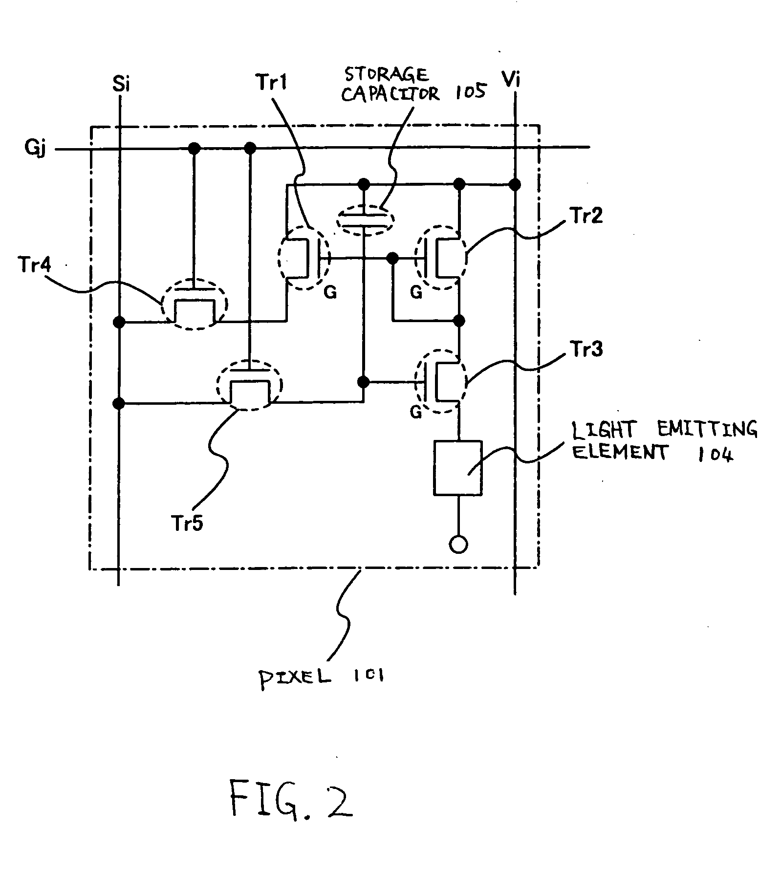
[0116] Taking a pixel shown in FIG. 2 for example, description on this example refers to a case in which the inverse biasing period Ti is made to appear based on a timing that differs from that shown in FIG. 4. Referring now to FIG. 5, a drive method according to this example is described below.

[0117]FIG. 5 exemplifies a timing chart of a voltage applied to individual scanning lines, a voltage applied to the power supply line, and a voltage fed to a light emitting element in a pixel (i, j) in this example. FIG. 5 exemplifies a case in which the transistors Tr1 Tr2 and Tr3 are composed of p-channel type TFTs, whereas the transistors Tr4 and Tr5 are both composed of n-channel type TFTs.

[0118] It is defined that the total length comprising the write in periods Ta1-Tan and the display periods Td1-Tdn corresponds to T_1 and a potential difference between the power supply line Vi and an opposing electrode of the light emitting element during the writing and display periods is expressed ...

example 2

[0120] Taking a pixel shown in FIG. 2 for example, description on this example refers to a case in which the inverse biasing period Ti is made to appear based on a timing that differs from those shown in FIGS. 4 and 5. Referring now to FIG. 6, a drive method according to this example is described below.

[0121]FIG. 6 exemplifies a timing chart of a voltage applied to individual scanning lines, a voltage applied to the power supply line, and a voltage fed to a light emitting element in a pixel (i, j) in this example. FIG. 6 exemplifies a case in which the transistors Tr1, Tr2 and Tr3 are all composed of p-channel type TFTs, whereas the transistors Tr4 and Tr5 are both composed of n-channel type TFTs.

[0122] In this example, immediately after termination of individual display periods Td1-Tdn, in other words, immediately after terminating individual sub-frame periods, the inverse biasing periods Ti1-Tin respectively appear. For example, while the m-th sub-frame period SFm remains (where...

example 3

[0124] Taking a pixel shown in FIG. 2 for example, description on this example refers to a case in which the inverse biasing period Ti is made to appear based on a timing that differs from those shown in FIGS. 4 to 6. Referring now to FIG. 7, a drive method according in this example is described below.

[0125]FIG. 7 exemplifies a timing chart of a voltage applied to individual scanning lines, a voltage applied to the power supply line, and a voltage fed to a light emitting element in a pixel (i, j) in this example. FIG. 7 exemplifies a case in which the transistors Tr1, Tr2 and Tr3 are all composed of p-channel type TFTs, whereas the transistors Tr4 and Tr5 are both composed of n-channel type TFTs.

[0126] In this example, immediately after termination of individual display periods Td1-Tdn, in other words, immediately after terminating individual sub-frame periods, the inverse biasing periods Ti1-Tin respectively appear. For example, while the m-th sub-frame period SFm remains (where ...


PUM


Abstract

By controlling the luminance of light emitting element not by means of a voltage to be impressed to the TFT but by means of controlling a current that flows to the TFT in a signal line drive circuit, the current that flows to the light emitting element is held to a desired value without depending on the characteristics of the TFT. Further, a voltage of inverted bias is impressed to the light emitting element every predetermined period. Since a multiplier effect is given by the two configurations described above, it is possible to prevent the luminance from deteriorating due to a deterioration of the organic luminescent layer, and further, it is possible to maintain the current that flows to the light emitting element to a desired value without depending on the characteristics of the TFT.

Description

BACKGROUND OF THE INVENTION [0001] 1. Field of the Invention [0002] The present invention relates to a light emitting panel in which a light emitting element formed on a substrate is enclosed between the substrate and a cover member. Also, the present invention relates to a light emitting module in which an IC or the like is mounted on the light emitting panel. Note that, in this specification, the light emitting panel and the light emitting module are generically called light emitting devices. The present invention further relates to a method of driving the light emitting device and an electronic appliance using the light emitting device. [0003] 2. Description of the Related Art [0004] A light-emitting element emits light by itself, and thus, has high visibility. The light-emitting element does not need a backlight necessary for a liquid crystal display device (LCD), which is suitable for a reduction of a light-emitting device in thickness. Also, the light-emitting element has no l...

Claims


Application Information

Patent Timeline
Patent Type & Authority Applications(United States)
IPC IPC(8): G09G3/20G09G3/30G09G3/22G09G3/32H01L51/50H05B33/14
CPCG09G3/2018H01L27/3244G09G3/22G09G3/3241G09G3/325G09G3/3283G09G2300/0426G09G2300/0814G09G2300/0842G09G2300/0861G09G2300/0866G09G2310/0256G09G2310/0262G09G2310/027G09G2320/0233G09G2320/043G09G2330/028G09G2330/04H01L27/15G09G2300/04H01L27/1255G09G3/2022G09G3/30H10K59/123H10K50/846H10K59/12H10K59/124H10K59/131H10K59/1213H10K59/1216H10K59/1315H10K59/1201H10K85/113H10K85/114H10K85/115H10K85/324H10K85/342H10K85/346H10K85/631H10K85/6574H10K2102/103H01L27/12H01L27/13H01L29/4908H01L29/66757H01L33/20H01L33/32G09G3/3233G09G3/3258G09G2310/0286G09G2310/0291G09G2310/08G09G2320/045H01L27/1285G09G3/3225G09G2330/045H01L27/124
Inventor YAMAZAKI, SHUNPEIAKIBA, MAIKOYAMA, JUN
Owner SEMICON ENERGY LAB CO LTD
Why Eureka
Try Eureka