Supercharge Your Innovation With Domain-Expert AI Agents!

Photo-sensor array with pixel-level signal comparison

a photosensor and array technology, applied in the field of photosensor arrays, can solve the problems of increasing cost, storing images, and digitally oriented application specific integrated circuit (asic) technologies, and achieve the effect of reducing the storage requirements of the overall image processing chip

Inactive Publication Date: 2005-05-19
MICROSOFT TECH LICENSING LLC
View PDF10 Cites 5 Cited by
  • Summary
  • Abstract
  • Description
  • Claims
  • Application Information

AI Technical Summary

Benefits of technology

[0010] A photo sensor pixel according to the invention provides DC Removal (DCR) and contrast enhancement signal processing in the analog domain at the pixel level. By performing DCR at the pixel level, separate (i.e., off-pixel) Analog to Digital Conversion (ADC) and DCR processing are no longer necessary. In one embodiment, each pixel cell generates a single bit of DCR processed (“DCRed”) image data. The pixel bit values can then be stored in memory for image correlation processing at any desired time. In other embodiments, one or more additional bits may be provided for each pixel. A two dimensional array of pixels according to the invention reduces the storage requirements of the overall image processing chip.
[0011] A pixel cell according to the invention allows reduction in the analog and digital circuitry of an array of pixel cells. The analog circuitry of the pixel also facilitates incorporation of an array of such pixels into newer digitally-oriented Application Specific Integrated Circuit (ASIC) technologies having lower supply voltages. A pixel cell according to the invention may also reduce chip cost and testing time. Moreover, the reduced design complexity of the pixel's analog circuitry is generally less sensitive to sub-threshold leakage and gate leakage sometimes associated with modem digital ASICs. The pixel cell may also consume less static supply current, allowing longer battery life when used in battery powered devices. Switching currents may also be reduced by operating at lower clock rates than those needed for traditional approaches such as, e.g., high-speed serial processing.

Problems solved by technology

This architecture is also susceptible to parasitic signal couplings, capacitor leakages and charge injections, and can only store an image without corruption for a relatively short time.
Moreover, this architecture presents problems with regard to digitally-oriented Application Specific Integrated Circuit (ASIC) technologies, which may involve high sub-threshold leakages and low power supply voltages.
This additional circuitry requires additional IC area, which increases cost.
Such parallel processing also increases power requirements.

Method used


Image

  • Photo-sensor array with pixel-level signal comparison
  • Photo-sensor array with pixel-level signal comparison
  • Photo-sensor array with pixel-level signal comparison

Examples


Embodiment Construction

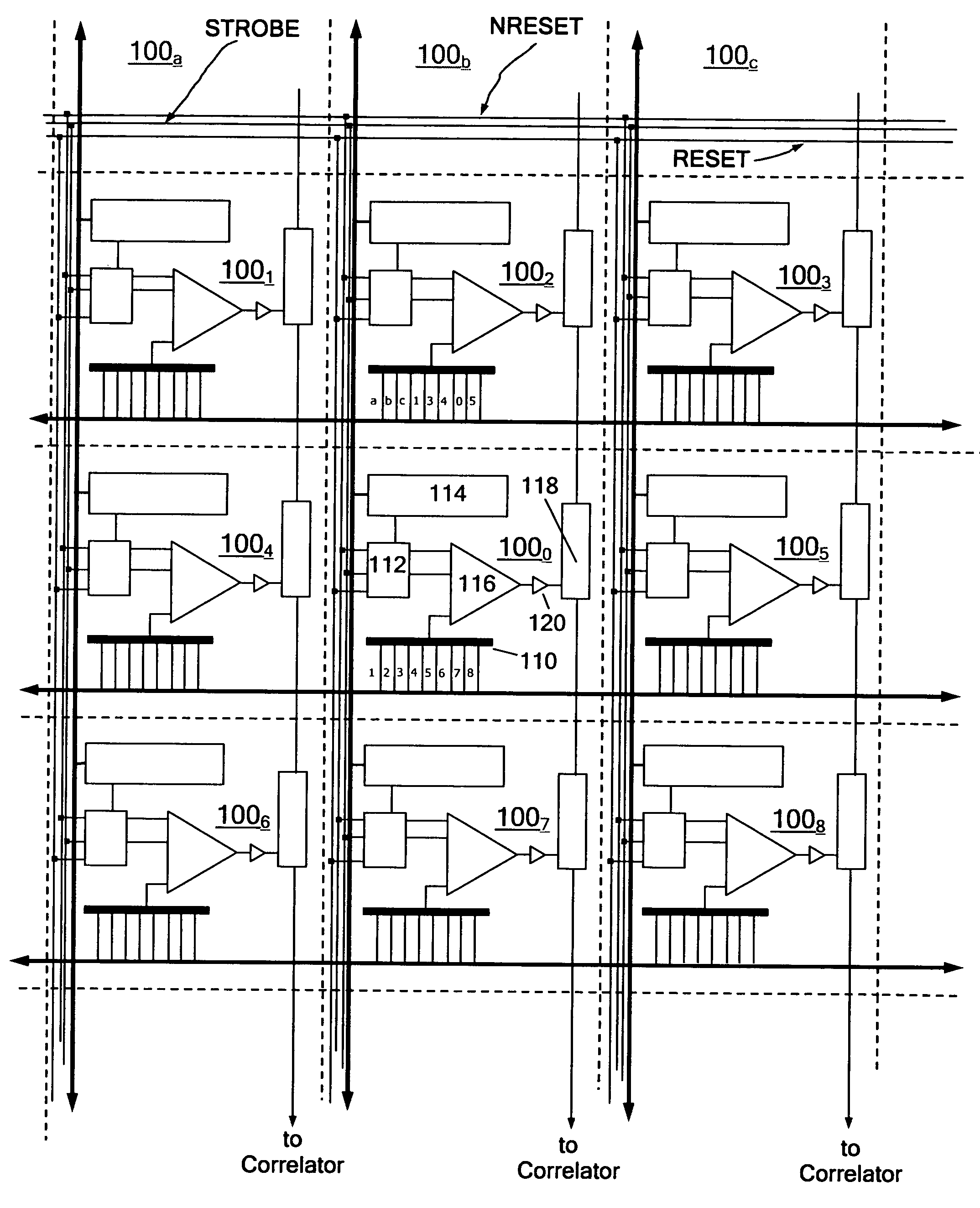
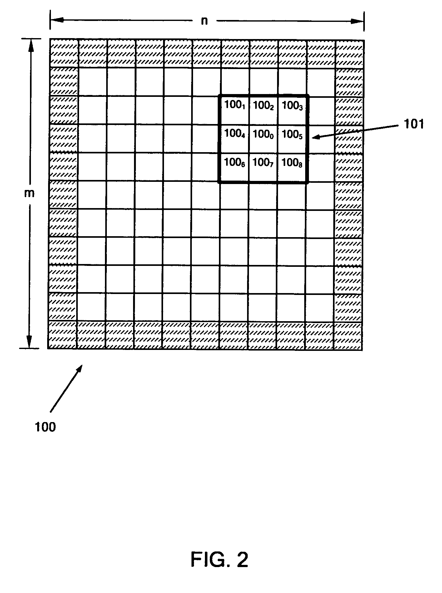
[0024]FIG. 2 is a block diagram of an array 100 having m rows and n columns of pixels. Array 100 (which could be formed as part of an integrated circuit) may form part of an electronic imager. In operation, array 100 may be configured to receive light reflected from a surface (or object), and thereby generate an image of the surface (or object). Array 100 is in communication with a controller device (e.g., additional circuitry on the same IC, not shown, and / or one or more separate processors, also not shown). Except as set forth below, the details of such components are not necessary for an understanding of the invention. Hardware and software (or firmware) suitable for implementation of a photo-sensor array of the invention will be apparent to one of ordinary skill in the art from the information provided herein.

[0025] Highlighted in FIG. 2 is a sub-array 101 of 9 contiguous pixels, labeled 1000 through 1008, at an arbitrary location within array 100. Except as set forth below, th...


PUM


Abstract

Pixels in an array of image sensor pixels contain photo-sensors. In response to illumination of a photo-sensor, an initial signal is generated. Multiple comparison signals are also generated based on the initial signal. One of the comparison signals remains internal to the pixel, and other comparison signals are transmitted to neighboring pixels. Within a pixel, the internal comparison signal is compared to a sum of comparison signals received from neighboring pixels. Based on the comparison, a data value may be latched and used for indicating a relative difference in pixel illumination.

Description

CROSS-REFERENCE TO RELATED APPLICATIONS [0001] This application is a continuation of U.S. patent application Ser. No. 10 / 283,264, filed Oct. 30, 2002 and titled “Photo-Sensor Array with Pixel-Level Signal Comparison,” now U.S. Pat. No. ______. Said application is hereby incorporated by reference in its entirety.FIELD OF THE INVENTION [0002] This invention relates to processing of output from photo-sensors as part of an imaging system, and more specifically, to an array of analog photo-sensors that provide DC removal processing at the pixel level. BACKGROUND OF THE INVENTION [0003] Photo-sensitive electronic components can be used to create electronic imaging systems, including systems for detecting and measuring motion. When used for motion detection, obtaining a highly detailed image of an area or object may be less important than determining whether a particular image reflects a change by comparison to a prior image. In turn, this may place higher importance upon contrast between ...

Claims


Application Information

Patent Timeline
Patent Type & Authority Applications(United States)
IPC IPC(8): G06F1/32G06F3/033G06F3/042H01L27/146H04N5/369
CPCG06F1/3203G06F1/3259G06F3/0421Y02B60/148H04N3/155Y02B60/1253H01L27/14609Y02D10/00
Inventor KNEE, DEREK L.OLIVER, THOMAS C.
Owner MICROSOFT TECH LICENSING LLC
Features
  • R&D
  • Intellectual Property
  • Life Sciences
  • Materials
  • Tech Scout
  • Unparalleled Data Quality
  • Higher Quality Content
  • 60% Fewer Hallucinations
Learn More