Pixel arranging apparatus, solid-state image sensing apparatus,and camera

a technology of solid-state image and arranging apparatus, which is applied in the field of solid-state image sensing apparatus, can solve problems such as degrading the image quality represented by the output image signal, and achieve the effect of reducing the number of pixels and high speed

Active Publication Date: 2005-05-19
PANASONIC SEMICON SOLUTIONS CO LTD
View PDF10 Cites 18 Cited by
  • Summary
  • Abstract
  • Description
  • Claims
  • Application Information

AI Technical Summary

Benefits of technology

[0010] The object of the present invention is therefore to provide a solid-state image sensing apparatus including a solid-state image sensing device which is capable of reducing the number of pixels to be processed, at least, in the horizontal direction, and outputting high-quality image signals at high speeds, without generating moire or false signals.

Problems solved by technology

Digital cameras use less pixels for shooting moving images than for taking still pictures, due to limited speeds at which image signals are output.
This generates moire or false signals, degrading the image quality represented by the output image signals.

Method used


Image

  • Pixel arranging apparatus, solid-state image sensing apparatus,and camera
  • Pixel arranging apparatus, solid-state image sensing apparatus,and camera
  • Pixel arranging apparatus, solid-state image sensing apparatus,and camera

Examples


Embodiment Construction

[0100] The following describes a preferred embodiment of the present invention, with reference to the attached drawings.

[0101] First, a solid-state image sensing device of the present invention will be described.

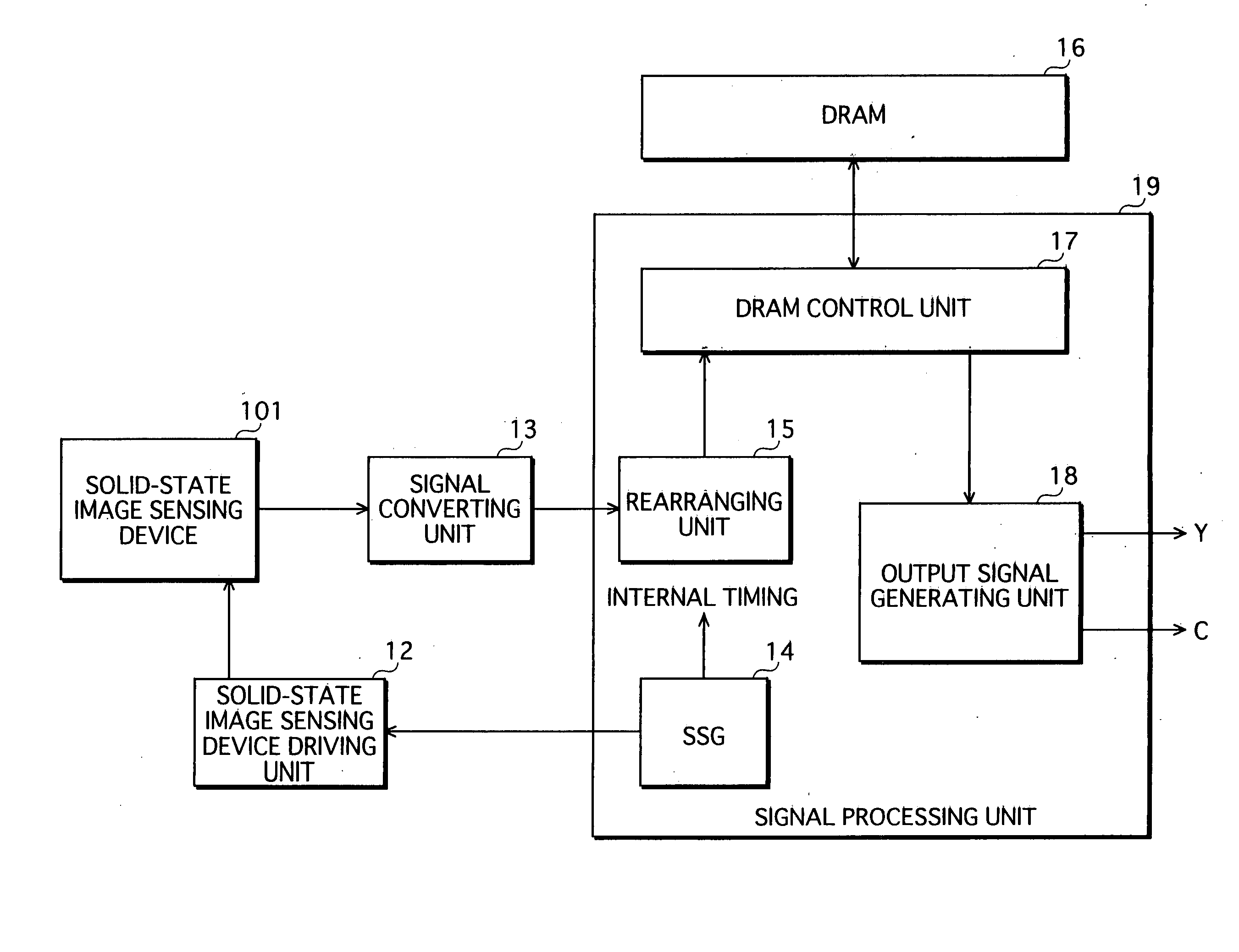
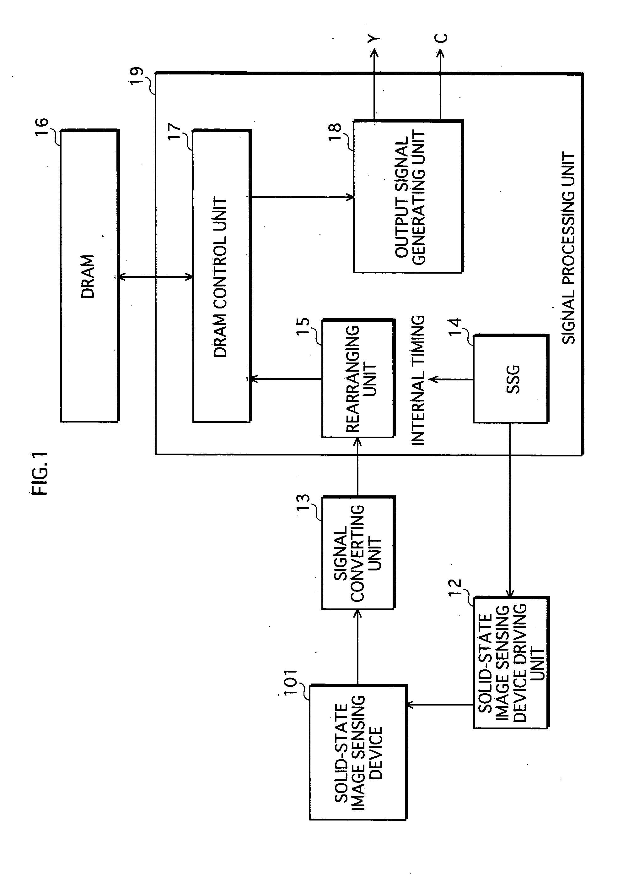
[0102]FIG. 19 shows a general construction of a solid-state image sensing device.

[0103] A solid-state image sensing device 101 adopts what is called “all-pixel simultaneously-and-independently reading” method, and includes light-to-electric conversion elements 102 arranged two-dimensionally in correspondence with the pixels, a vertical transfer unit 103, and a horizontal transfer unit 104. Also, the vertical transfer unit 103 is composed of a plurality of transfer columns that align horizontally, and a plurality of vertical transfer elements constitute each of the transfer columns.

[0104] The light-to-electric conversion elements 102 are photodiodes.

[0105] The light-to-electric conversion elements 102 are attached with color filters of red (R), green (G), and blue (B) th...


PUM


Abstract

A solid-state image sensing apparatus including a solid-state image sensing device and a signal processing circuit. The solid-state image sensing device includes: a vertical transfer unit, composed of transfer columns corresponding to columns of the light-to-electric conversion elements, operable to transfer, in a vertical direction, signal charges read out from the light-to-electric conversion elements; a horizontal transfer unit operable to receive the signal charges from the vertical transfer unit and transfer them in a horizontal direction. The signal processing circuit converts the signal charges from the horizontal transfer unit into pixel data, and rearranges it into a two-dimensional array. In the rearrangement, the signal processing circuit, per transfer of one piece of pixel data, cyclically selects a line memory out of three line memories, writes a piece of pixel data into the selected line memory, or reads a row of pixel data from the selected line memory.

Description

[0001] This application is based on applications No. 2003-365225 and 2004-143480 filed in Japan, the contents of which are hereby incorporated by reference. BACKGROUND OF THE INVENTION [0002] (1) Field of the Invention [0003] The present invention relates to a solid-state image sensing apparatus composed of a solid-state image sensing device, which converts received light into electric signals, and a signal processing circuit.[0004] (2) Description of the Related Art [0005] One of most eagerly developed apparatuses in recent years might be solid-state image sensing apparatuses, which include a solid-state image sensing device for converting received light into electric signals, and a signal processing circuit for converting the electric signals into image signals. [0006] The solid-state image sensing apparatuses are largely used in digital cameras, such as digital still cameras and digital video cameras. There has always been a strong demand for improving image quality of digital ca...

Claims


Application Information

Patent Timeline
Patent Type & Authority Applications(United States)
IPC IPC(8): H01L27/148H04N3/15H04N5/21H04N9/04
CPCH04N9/045H04N3/1562H04N25/445H04N25/40H04N25/53H04N23/10
Inventor SHIMAZU, YOSHIHISANAGAYOSHI, RYOUICHIFUJII, TOSHIYANAKASHIMA, TOSHIYUKIHATANO, TOSHINOBUKAJIWARA, JUNARAKAWA, KENJIKOGISHI, TOSHIYA
Owner PANASONIC SEMICON SOLUTIONS CO LTD
Why Eureka
Try Eureka