Ternary content addressable memory (TCAM) cells with small footprint size and efficient layout aspect ratio

a content addressable memory and layout aspect ratio technology, applied in the field of integrated circuit memory devices, can solve the problems of large pmos transistors that increase the overall unit cell size, and achieve the effects of enhancing scalability and uniformity of wiring pitch, reducing the size of layout footprint, and efficient layout aspect ratio

Inactive Publication Date: 2005-06-23
AVAGO TECH INT SALES PTE LTD
View PDF19 Cites 118 Cited by
  • Summary
  • Abstract
  • Description
  • Claims
  • Application Information

AI Technical Summary

Benefits of technology

[0006] Embodiments of the present invention include ternary CAM cells having extremely small layout footprint size and efficient layout aspect ratios that enhance scalability and uniformity of wiring pitch. The ternary CAM cells also have high degrees of symmetry that facilitate extensive sharing of vias between transistor-equivalent half-cells. These shared vias provide electrical interconnects between terminals of the CAM cell transistors and bit, data and match lines. Accordingly, when the CAM half-cells are joined together on all four sides to form a large CAM array, a low per cell via count can be achieved.
[0008] The first pair of cross-coupled inverters include a first inverter having a first PMOS pull-up transistor and a first NMOS pull-down transistor therein, and a second inverter having a second PMOS pull-up transistor and a second NMOS pull-down transistor therein. To facilitate high cell density, the first and second NMOS pull-down transistors are positioned so that they extend between the first and second PMOS pull-up transistors (on one side) and the first half of the 4T compare circuit (on an opposite side). The second pair of cross-coupled inverters include a second pair of PMOS pull-up transistors and a second pair of NMOS pull-down transistors, which extend between the second pair of PMOS pull-up transistors and the second half of the 4T compare circuit.
[0010] To achieve high degrees of scalability and support relatively uniform horizontal and vertical wiring pitches, a width / height aspect ratio of the ternary CAM cell is approximately square. In some embodiments, the width / height aspect ratio may be in a range from between about 1.08 and about 1.20. High density layouts can also be achieved by placing and orienting the MOS transistors of a CAM cell in orthogonal x and y directions that achieve a high packing density. In particular, a ternary CAM cell can be achieved having a footprint in a range from between about 3.0 μm2 and about 3.6 μm2.

Problems solved by technology

Unfortunately, because PMOS transistors typically have lower mobility relative to equivalently-sized NMOS transistors, using PMOS transistors as access transistors within an SRAM cell may require relatively large PMOS transistors that increase overall unit cell size.

Method used


Image

  • Ternary content addressable memory (TCAM) cells with small footprint size and efficient layout aspect ratio
  • Ternary content addressable memory (TCAM) cells with small footprint size and efficient layout aspect ratio
  • Ternary content addressable memory (TCAM) cells with small footprint size and efficient layout aspect ratio

Examples


Embodiment Construction

[0019] The present invention now will be described more fully herein with reference to the accompanying drawings, in which preferred embodiments of the invention are shown. This invention may, however, be embodied in many different forms and should not be construed as being limited to the embodiments set forth herein; rather, these embodiments are provided so that this disclosure will be thorough and complete, and will fully convey the scope of the invention to those skilled in the art. Like reference numerals refer to like elements throughout and signal lines and signals thereon may be referred to by the same reference characters. Signals may also be synchronized and / or undergo minor boolean operations (e.g., inversion) without being considered different signals. The suffix B (or prefix symbol “ / ”) to a signal name may also denote a complementary data or information signal or an active low control signal, for example.

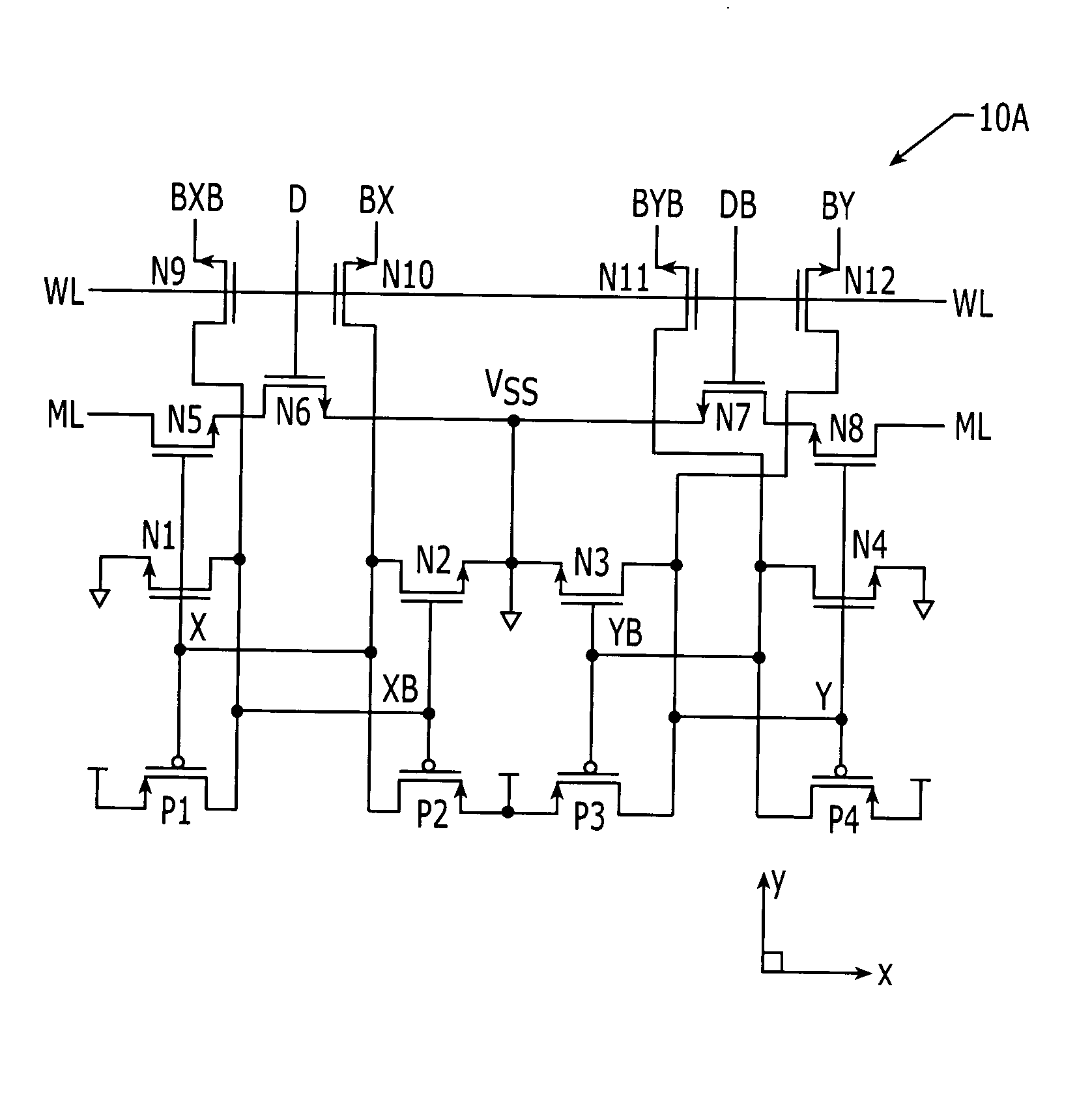
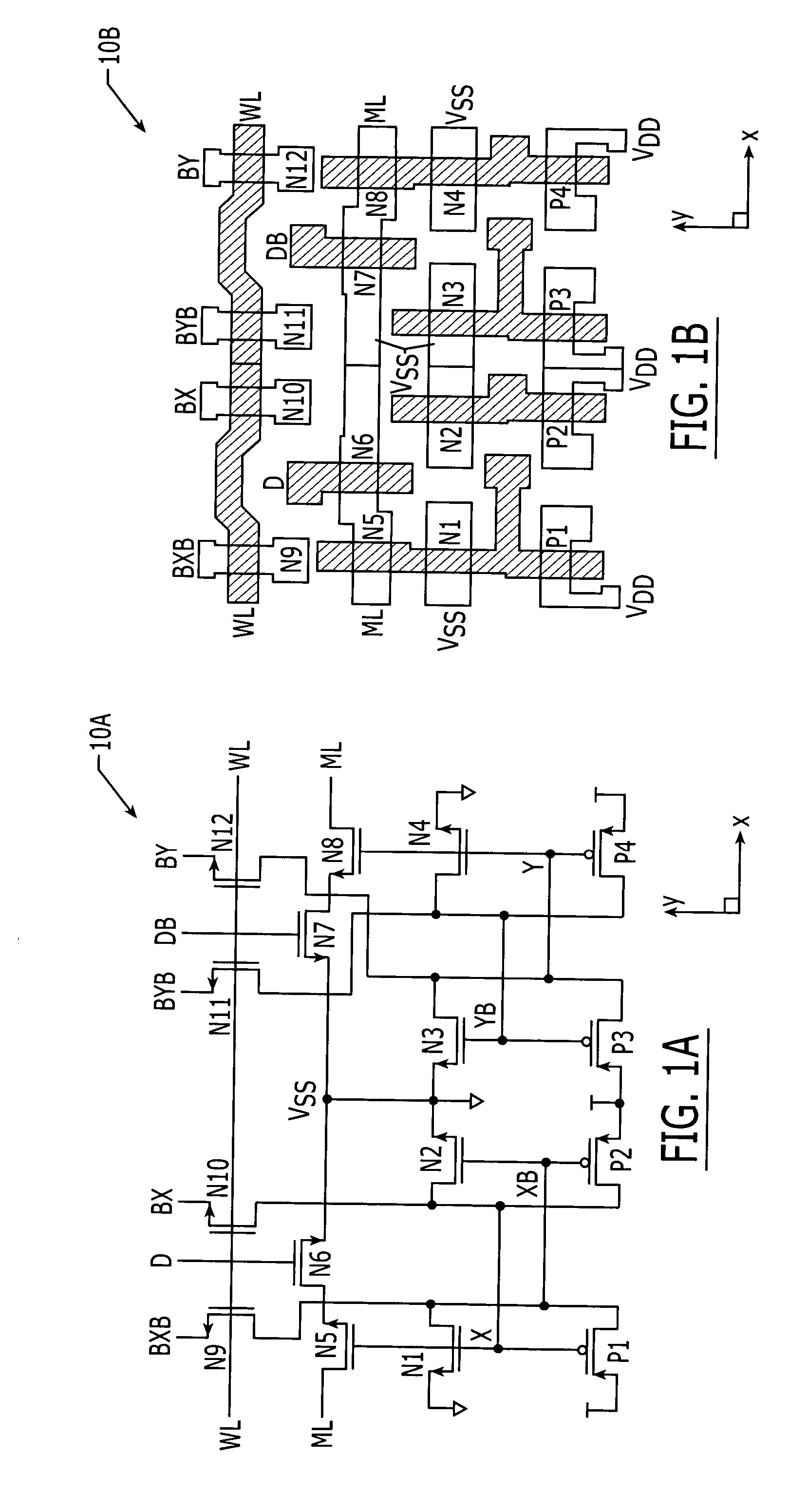
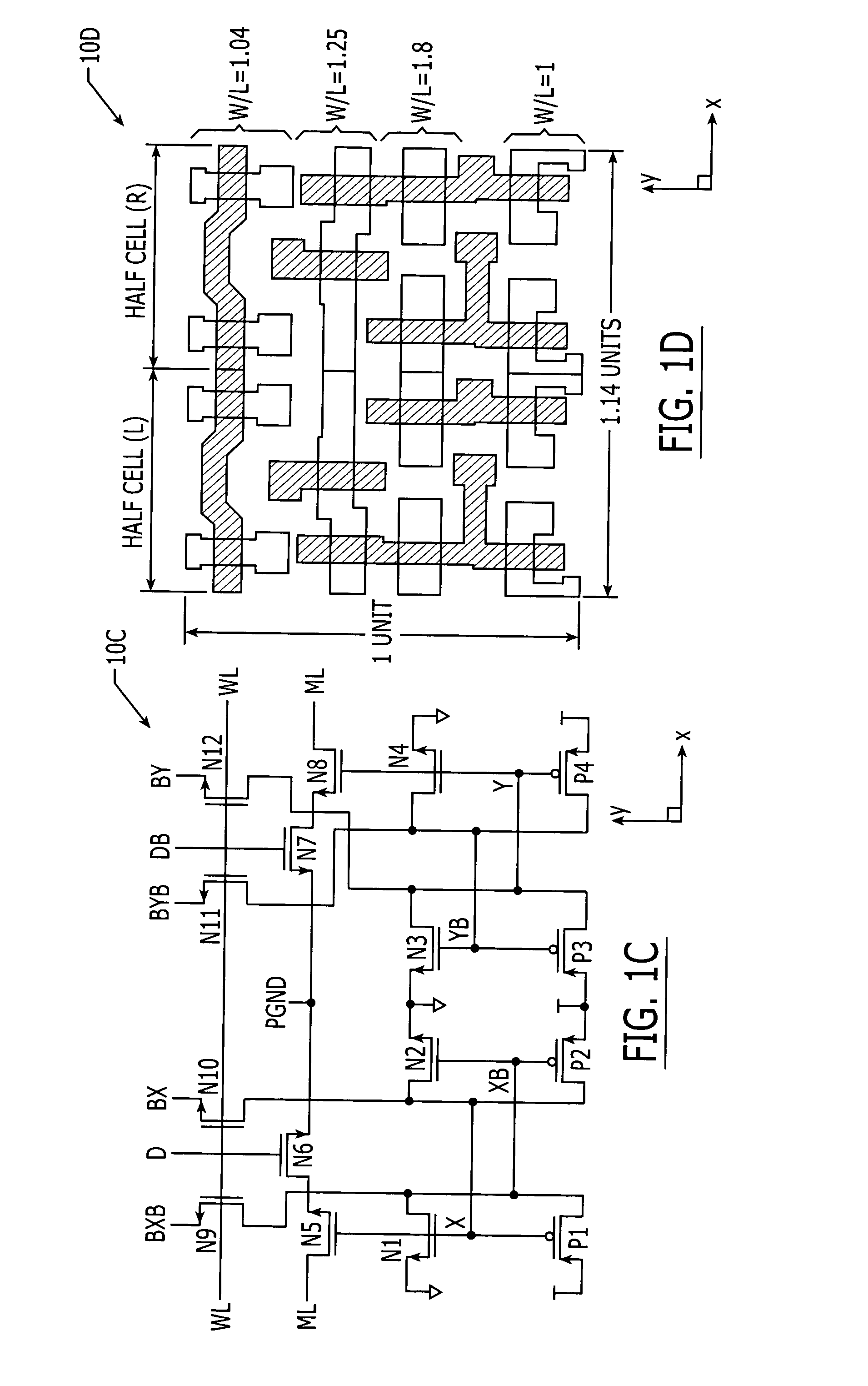
[0020] Referring now to FIG. 1A, an electrical schematic of a te...


PUM


Abstract

Ternary CAM cells are provided that have extremely small layout footprint size and efficient layout aspect ratios that enhance scalability. The cells also have high degrees of symmetry that facilitate high yield interconnections to bit, data and match lines. A 16T ternary CAM cell includes first and second pairs of access transistors that extend adjacent a first side of the cell, and first and second pairs of cross-coupled inverters that extend adjacent a second side of the cell. First and second halves of a 4T compare circuit are also provided. The first half of the 4T compare circuit is positioned so that is extends between the first pair of access transistors and the first pair of cross-coupled inverters. Similarly, the second half of the 4T compare circuit is positioned so that it extends between the second pair of access transistors and the second pair of cross-coupled inverters.

Description

FIELD OF THE INVENTION [0001] The present invention relates to integrated circuit memory devices and, more particularly, to content addressable memory (CAM) devices. BACKGROUND OF THE INVENTION [0002] In many memory devices, including random access memory (RAM) devices, data is typically accessed by supplying an address to an array of memory cells and then reading data from the memory cells that reside at the supplied address. However, in content addressable memory (CAM) devices, data within a CAM array is not accessed by initially supplying an address, but rather by initially applying data (e.g., search words) to the array and then performing a search operation to identify one or more entries within the CAM array that contain data equivalent to the applied data and thereby represent a “match” condition. In this manner, data is accessed according to its content rather than its address. Upon completion of the search operation, the identified location(s) containing the equivalent data...

Claims


Application Information

Patent Timeline
Patent Type & Authority Applications(United States)
IPC IPC(8): G11C15/04
CPCG11C15/04
Inventor YEN, TING-PWUPARK, KEE
Owner AVAGO TECH INT SALES PTE LTD
Why Eureka
Try Eureka