Liquid crystal display device and fabricating method thereof

a technology of liquid crystal display and fabrication method, which is applied in the direction of instruments, non-linear optics, optics, etc., can solve the problems of affecting the performance reducing the polarizing efficiency of the lcd device, etc., to increase the polarizing efficiency reduce the profile and increase the flexibility of the liquid crystal display panel

Inactive Publication Date: 2005-06-30
LG DISPLAY CO LTD
View PDF6 Cites 14 Cited by
  • Summary
  • Abstract
  • Description
  • Claims
  • Application Information

AI Technical Summary

Benefits of technology

[0017] An object of the present invention is to provide a liquid crystal display (LCD) device and a fabricating method thereof that can increase polarizing efficiency of a liquid crystal display panel.
[0018] Another object of the present invention is to provide a liquid crystal display (LCD) device and a fabricating method thereof that can increase flexibility of a liquid crystal display panel.
[0019] Another object of the present invention is to provide a liquid crystal display (LCD) device and a fabricating method thereof that can reduce the profile of a liquid crystal display panel.
[0020] Another object of the present invention is to provide a liquid crystal display (LCD) device and a fabricating method thereof that makes a liquid crystal display panel more resistant to deformation by heat and moisture.

Problems solved by technology

Therefore, polarizing efficiency of the LCD device is reduced.
Thus, the performance of the liquid crystal panel can be adversely affected by heat and moisture.

Method used


Image

  • Liquid crystal display device and fabricating method thereof
  • Liquid crystal display device and fabricating method thereof
  • Liquid crystal display device and fabricating method thereof

Examples


first embodiment

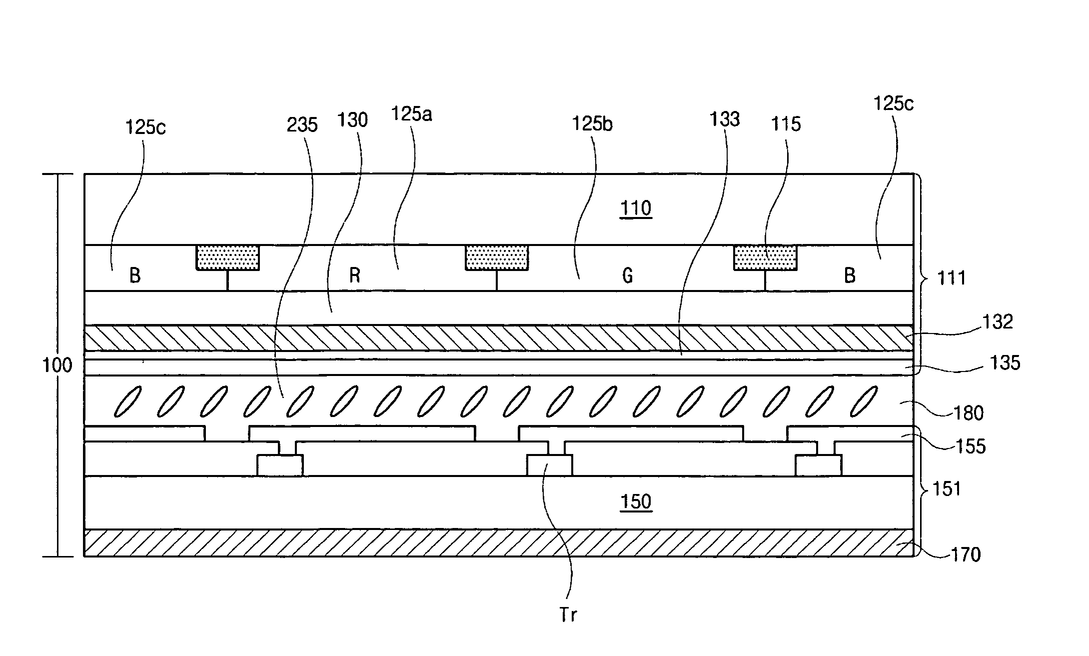
[0036]FIG. 5 is a cross-sectional view of a liquid crystal panel according to the present invention. As shown in FIG. 5, a liquid crystal panel 100 includes an upper substrate 111 as a color filter substrate, a lower substrate 151 as an array substrate, and a liquid crystal material 180 interposed between the upper and lower substrates 111 and 151. Inner surfaces of the upper substrate 111 and the lower substrate 151 face each other. A polarizing film 170 is attached on the outer surface of the lower substrate 151.

[0037] The lower substrate 151 includes a first substrate 150. A thin film transistor Tr is on the inner surface of the first substrate 150. A pixel electrode 155 is connected with the thin film transistor Tr. Although not shown in FIG. 5, the lower substrate 151 also includes a gate line and a data line crossing each other. The thin film transistor Tr is disposed adjacent to where the gate line and the data line cross. The thin film transistor Tr includes a gate electrode...

second embodiment

[0050] the present invention relates to an in-plane switching (IPS) mode liquid crystal display (LCD) device. The IPS mode LCD device includes a color filter substrate having a color filter pattern, an array substrate having a thin film transistor, and a liquid crystal interposed between the color filter substrate and the array substrate. A pixel electrode and a common electrode are disposed on the array substrate. The pixel electrode and the common electrode are parallel to and spaced apart from each other within a pixel region. Alignment of liquid crystal molecules is changed by the in-plane electric field induced between the common electrode and the pixel electrode. Therefore, the IPS mode LCD has a wide viewing-angle, about 80 degrees˜85 degrees.

[0051]FIG. 7 is a cross-sectional view of a liquid crystal panel according to a second embodiment of the present invention. In the second embodiment, explanations of parts similar to parts in the first embodiment will be omitted. As show...


PUM

PropertyMeasurementUnit
thicknessaaaaaaaaaa
thicknessaaaaaaaaaa
thicknessaaaaaaaaaa

Abstract

A liquid crystal display (LCD) device includes: first and second substrates, inner surfaces of the first and second substrates facing each other; gate and data lines crossing each other to define a pixel region on the inner surface of the first substrate; a thin film transistor at the crossing of the gate and data lines; a pixel electrode connected with the thin film transistor; a color filter pattern on the inner surface of the second substrate; a first polarizing layer between the first and second substrates and adjacent to the color filter pattern; and a liquid crystal material between the first and second substrates.

Description

[0001] The present invention claims the benefit of Korean Patent Application No. 2003-0101675 filed in Korea on Dec. 31, 2003, which is hereby incorporated by reference for all purposes as if fully set forth herein. BACKGROUND OF THE INVENTION [0002] 1. Field of the Invention [0003] The present invention relates to a liquid crystal display (LCD) device, and more particularly, to an LCD device and fabricating method thereof. [0004] 2. Discussion of the Related Art [0005] Until recently, display devices have typically used cathode-ray tubes (CRTs). Presently, many efforts are being made to study and develop various types of flat panel displays, such as liquid crystal display (LCD) devices, plasma display panels (PDPs), field emission displays, and electro-luminescence displays (ELDs), as a substitute for CRTs. Of these flat panel displays, LCD devices have many advantages, such as high resolution, light weight, thin profile, compact size, and low voltage power supply requirements. [00...

Claims


Application Information

Patent Timeline
Patent Type & Authority Applications(United States)
IPC IPC(8): G02F1/1335G02F1/1343
CPCG02F2001/133565G02F1/133528G02F1/133565G02F1/1335
Inventor YOON, SUNGHOE
Owner LG DISPLAY CO LTD
Why Eureka
Try Eureka