Strobe light control circuit and IGBT device

a control circuit and strobe light technology, applied in the field of strobe light control circuits, can solve the problems of easy noise, easy noise, and easy failure of the strobe light to light up and malfunction, and achieve the effect of preventing light emission failure, high noise immunity, and preventing nois

Inactive Publication Date: 2005-07-07
RENESAS ELECTRONICS CORP
View PDF11 Cites 2 Cited by
  • Summary
  • Abstract
  • Description
  • Claims
  • Application Information

AI Technical Summary

Benefits of technology

[0018] An object of the present invention is to provide an IGBT device having high noise immunity, capable of preventing light emission failure and a malfunction in a strobe light control circuit even with a low supply voltage.
[0021] A voltage signal applied by the drive circuit between the gate terminal and the second emitter terminal is applied between the gate electrode and emitter electrode with its amplitude unchanged. Therefore, it becomes unnecessary to provide a large margin for the amplitude of a voltage signal for driving the IGBT device, which allows the amplitude of the voltage signal generated by the drive circuit to be kept smaller than in a conventional strobe light control circuit. As a result, this contributes to reduced power requirements in, e.g., digital cameras in which strobe light control circuits are used. Further, the drive voltage for the IGBT chip can be set high to a certain degree even in the case where a supply voltage is low and the output voltage of the drive circuit is kept low, causing the output voltage of the drive circuit to be kept low. This makes it possible to suppress degradation of the IGBT chip in noise immunity.

Problems solved by technology

As a result, light emission failure of the strobe light and a malfunction due to noise easily occur.
Potential variations at the emitter electrode due to load current variations (di / dt) in an inverter circuit and wiring inductance of the IGBT module cause the overcurrent protection circuit to malfunction.
It is thus becoming difficult to implement the method of increasing a margin for a voltage signal.
However, merely decreasing a drive voltage for the IGBT chip disadvantageously degrades the IGBT chip itself in noise immunity.

Method used


Image

  • Strobe light control circuit and IGBT device
  • Strobe light control circuit and IGBT device
  • Strobe light control circuit and IGBT device

Examples


first preferred embodiment

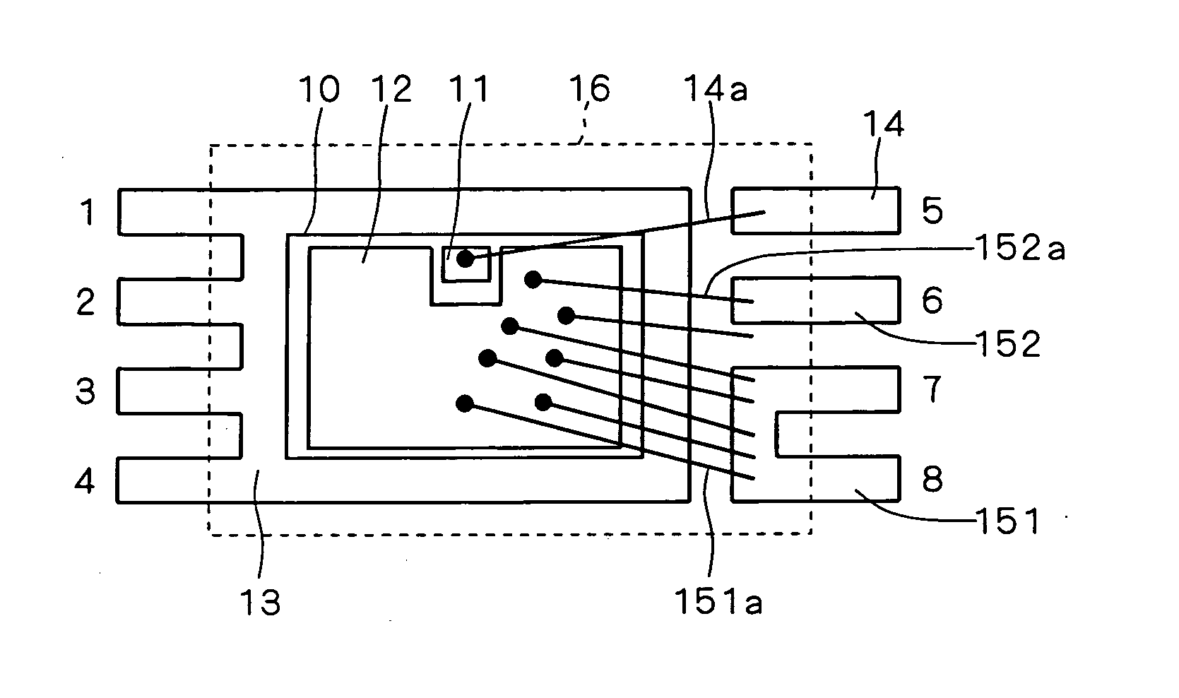
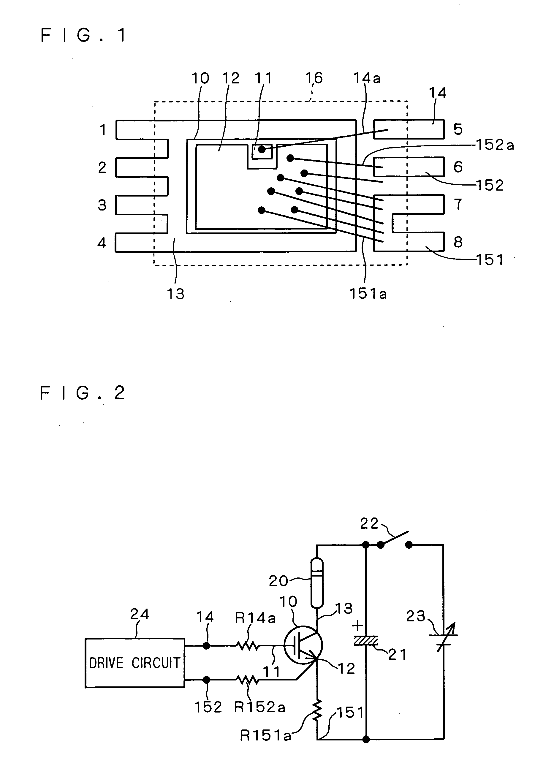
[0028]FIG. 1 is a top view showing the configuration of an IGBT device according to a first preferred embodiment of the present invention. An IGBT device in TSSOP-8 package is also illustrated here. Components having the same functions as those shown in FIG. 4 are designated by the same reference characters, detailed explanation of which is thus omitted.

[0029] As shown in FIG. 1, the IGBT device has, as external connection terminals for the emitter electrode 12, a first emitter terminal 151 for connecting a light emitter in a strobe light control circuit to the emitter electrode 12 and a second emitter terminal 152 for connecting a drive circuit for driving the IGBT device to the emitter electrode 12.

[0030] The first emitter terminal 151 is connected to the emitter electrode 12 via wires 151a, while the second emitter terminal 152 is connected to the emitter electrode 12 via a wire 152a. That is, the first and second emitter terminals 151 and 152 are connected individually to the ...

second preferred embodiment

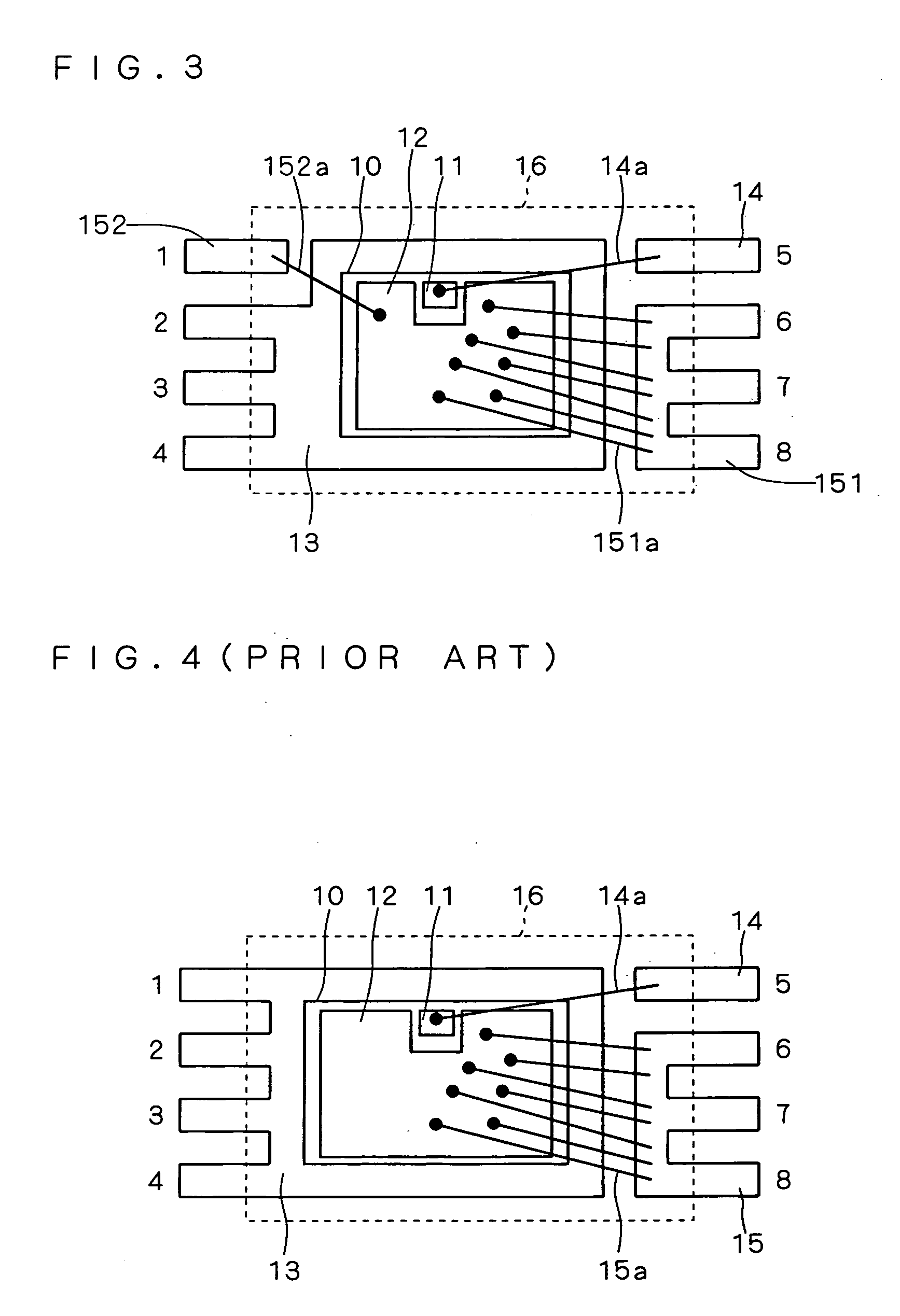
[0042] As described, when the IGBT device according to the present invention is in the ON state, a large current flows through the wires 151a. As is apparent from FIG. 1, the first emitter terminal 151 in the first preferred embodiment is smaller than the conventional emitter terminal 15 shown in FIG. 4. Thus, the number of wires 151a that can be used for bonding is inevitably smaller than that of conventional wires 15a. As a result, this disadvantageously increases the on-state resistance (conduction resistance) of the IGBT device and decreases the current-carrying capacity, thus causing a reduction in reliability of the IGBT device. Accordingly, an IGBT device that can avoid such drawbacks will be proposed in the present embodiment.

[0043]FIG. 3 is a top view showing the configuration of an IGBT device according to a second preferred embodiment of the present invention. An IGBT device in TSSOP-8 package is also illustrated here. Components having the same functions as those shown ...


PUM


Abstract

As external connection terminals for an emitter electrode (12) of an IGBT chip, a first emitter terminal (151) for electrically connecting a light emitter in a strobe light control circuit to the emitter electrode (12) and a second emitter terminal (152) for connecting a drive circuit for driving an IGBT device to the emitter electrode (12) are provided. The first emitter terminal (151) and the second emitter terminal (152) are individually connected to the emitter terminal (12) by wire bonding.

Description

BACKGROUND OF THE INVENTION [0001] 1. Field of the Invention [0002] The present invention relates to a strobe light control circuit for a camera, and more particularly to an insulated gate bipolar transistor (IGBT) for a strobe light. [0003] 2. Description of the Background Art [0004] Insulated gate bipolar transistors (hereinafter referred to as “IGBT”) in 8-pin IC packages, for example, are widely employed as semiconductor elements for controlling strobe lights of cameras. [0005]FIG. 4 is a top view showing the configuration of a conventional IGBT device for controlling a strobe light. A common IGBT device in TSSOP-8 package is illustrated here as an example. A semiconductor chip (IGBT chip) 10 has a gate electrode 11 and an emitter electrode 12 formed on its upper surface and a collector electrode (not shown) formed on its lower surface. The IGBT chip 10 is mounted on a lead frame 13 and bonded thereto by solder or the like such that the collector electrode formed on its lower su...

Claims


Application Information

Patent Timeline
Patent Type & Authority Applications(United States)
IPC IPC(8): G03B15/05G03B15/02H01L23/48H01L23/495H01L29/423H01L29/78H05B41/30H05B41/32
CPCH01L23/49562H01L2224/06051H01L24/06H01L24/48H01L24/49H01L25/167H01L29/4238H01L2224/04042H01L2224/05552H01L2224/05599H01L2224/0603H01L2224/48247H01L2224/48465H01L2224/49111H01L2224/49431H01L2224/85399H01L2924/01002H01L2924/01004H01L2924/01006H01L2924/01082H01L2924/014H01L2924/19041H01L2924/30107H01L2924/3011H05B41/32H01L24/05H01L2924/1305H01L2924/00014H01L2924/01033H01L2924/13055H01L2224/45099H01L2924/00H01L2924/00012H01L2924/181H01L2924/10161H01L2224/05553
Inventor KAWANO, MAKOTO
Owner RENESAS ELECTRONICS CORP
Why Eureka
Try Eureka