Electronic component manufacturing apparatus, electronic component manufacturing method, and electronic component

a technology of electronic components and manufacturing methods, applied in the direction of photomechanical equipment, instruments, originals for photomechanical treatment, etc., can solve the problem of insufficient strength of the resin layer in its entirety

Inactive Publication Date: 2005-07-14
KK TOSHIBA
View PDF10 Cites 18 Cited by
  • Summary
  • Abstract
  • Description
  • Claims
  • Application Information

AI Technical Summary

Benefits of technology

[0012] Further, according to an aspect of the present invention, there is provided a method of manufacturing an electronic component, comprising: a dissolving step to heat and dissolve an insulating pattern formed of thermosetting resin and formed on a substrate; a metal particulate spraying step to spray metal particulates over said substrate having the insulating pattern which is dissolved, and attach the metal particulates on the dissolved insulating pattern; a curing step to heat and cure said insulating pattern, which has said metal particulates attached thereon, and fix said metal particulates on said insulating pattern; and a metal particulate eliminating step to eliminate the metal particulates attached on the surface of the substrate excluding said insulating pattern.
[0013] Furthermore, according to an aspect of the present invention, there is provided a method of manufacturing an electronic component, comprising: a liquid attaching step to attach liquid, containing a specific ratio of metal particulates and vaporizing at a specific temperature, on a substrate having an insulating pattern formed of thermosetting resin; a heating step to heat said insulating pattern to which said liquid is attached, vaporize said liquid and at the same time dissolve the insulating pattern, and fix said metal particulates on the insulating pattern; and a metal particulate eliminating step to eliminate the metal particulates attached on the substrate excluding said insulating pattern.

Problems solved by technology

However, because of the inclusion of the metal particulates in the metal-particulate-containing resin layer formed by dissolving plural particles of the insulating resin particles attaching metal particulates over the surface thereof, the adhesiveness of the interface between the contained metal particulates and the resin affects the material to easily crack which is a cause of a damage.
As a result, the strength of the resin layer in its entirety becomes insufficient.

Method used


Image

  • Electronic component manufacturing apparatus, electronic component manufacturing method, and electronic component
  • Electronic component manufacturing apparatus, electronic component manufacturing method, and electronic component
  • Electronic component manufacturing apparatus, electronic component manufacturing method, and electronic component

Examples


Embodiment Construction

[0023] In the following, an embodiment of the present invention will be described with reference to the drawings.

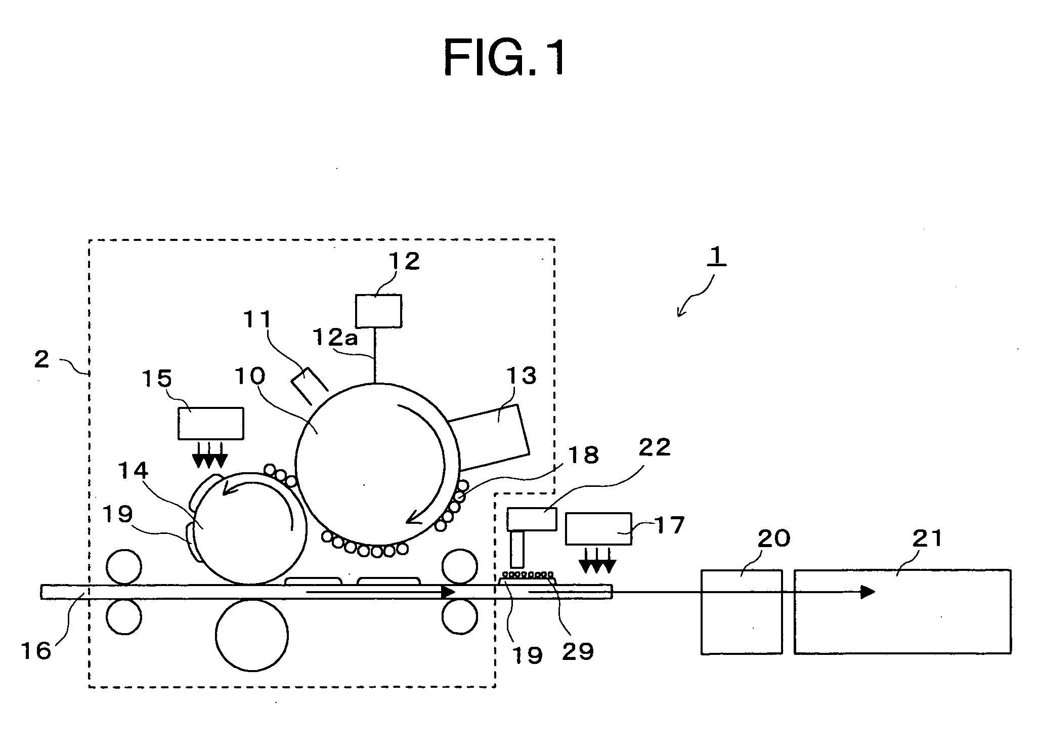
[0024]FIG. 1 shows an overview of a configuration of an electronic component manufacturing apparatus 1 according to an embodiment of the present invention.

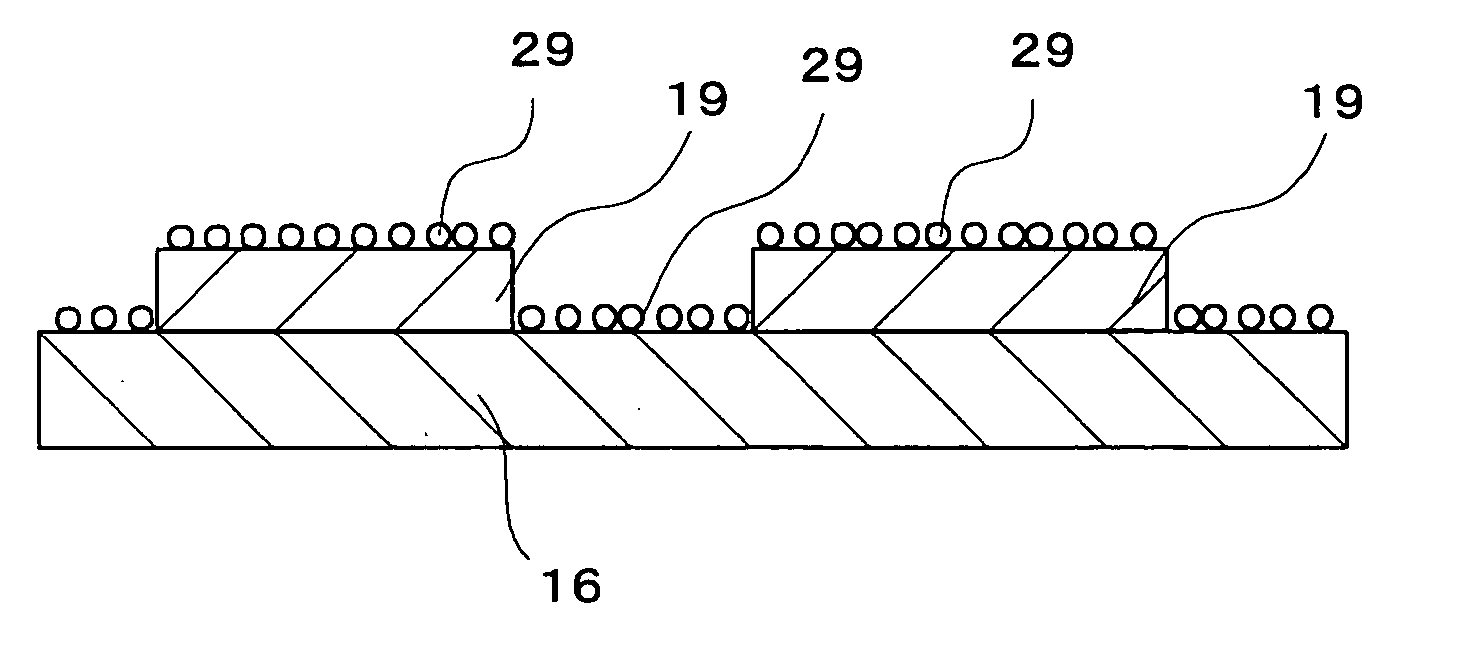
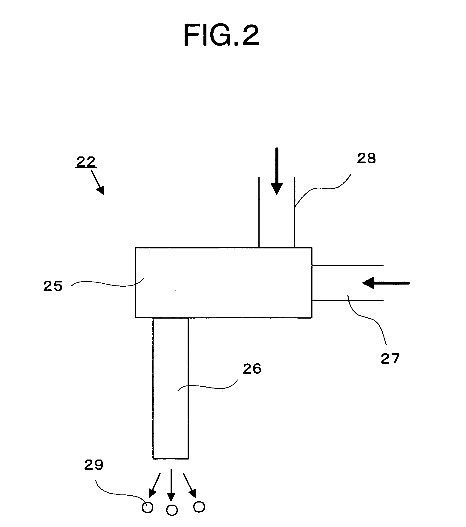
[0025] The electronic component manufacturing apparatus 1 according to the embodiment of the present invention consists mainly of: a resin pattern forming apparatus 2 to form, on a substrate 16, a resin pattern serving as an insulating pattern; a metal particulate attaching apparatus 22 to attach metal particulates 29 on a resin layer 19 formed on the substrate 16; a heating apparatus 17 to heat the resin layer 19; a metal particulate eliminating apparatus 20 to eliminate metal particulates 29 attached on the substrate 16; and an electroless plating tank 21 to form a metal conductor layer 19, which has metal particulates 29 attached thereon.

[0026] Here, FIG. 1 shows, as an example of the resin pattern forming apparat...


PUM

PropertyMeasurementUnit
sizeaaaaaaaaaa
sizeaaaaaaaaaa
sizeaaaaaaaaaa

Abstract

There are provided a metal particulate spraying step to spray metal particulates over a substrate having an insulating pattern formed of thermosetting resin, a heating step to heat and dissolve the resin pattern and fix the metal particulates on the resin pattern, and a metal particulate eliminating step to eliminate metal particulates attached on the surface of the substrate excluding the resin pattern.

Description

CROSS REFERENCE TO THE INVENTION [0001] This application is based upon and claims the benefit of priority from the prior Japanese Patent Application No. 2004-05046 filed on Jan. 13, 2004; the entire contents of which are incorporated herein by reference. BACKGROUND OF THE INVENTION [0002] 1. Field of the Invention [0003] The present invention relates to an electronic component manufacturing apparatus, an electronic component manufacturing method, and an electronic component. [0004] 2. Description of the Related Art [0005] In recent years, electrophotographic methods to form an electronic circuit pattern on a substrate are developed. In the electrophotographic method to form an electronic circuit pattern, an electrostatic latent image of a specific pattern is formed on a photoreceptor, and insulating resin particles, over the surface of each of which metal particulates adhere, are electrostatically attached on the electrostatic latent image to form a visible image, which is then tran...

Claims


Application Information

Patent Timeline
Patent Type & Authority Applications(United States)
IPC IPC(8): H05K3/18G03F7/00G03G16/00G03G17/08H01L21/447H01L21/48H05K3/10
CPCH01L21/4857H01L21/4867H05K2203/1105H05K2203/0522H05K3/102G03G16/00
Inventor YAMAGUCHI, NAOKOAOKI, HIDEOTAKUBO, CHIAKI
Owner KK TOSHIBA
Why Eureka
Try Eureka