Flip chip packaging process employing improved probe tip design

a technology of probe tip and flip chip, which is applied in the direction of material analysis, instruments, semiconductor/solid-state device details, etc., can solve the problems of over-mentioned flip-chip packaging process flow, high risk for ic chip manufacturers, and delay of important yield feedback information for 5 to 7 days, so as to reduce the entire process time for packaging and reduce yield feedback time

a technology of probe tip and flip chip, which is applied in the direction of material analysis, instruments, semiconductor/solid-state device details, etc., can solve the problems of over-mentioned flip-chip packaging process flow, high risk for ic chip manufacturers, and delay of important yield feedback information for 5 to 7 days, so as to reduce the entire process time for packaging and reduce yield feedback time

US20050164428A1Inactive Publication Date: 2005-07-28UNITED MICROELECTRONICS CORP

Image

  • Flip chip packaging process employing improved probe tip design
  • Flip chip packaging process employing improved probe tip design
  • Flip chip packaging process employing improved probe tip design

Examples


Embodiment Construction

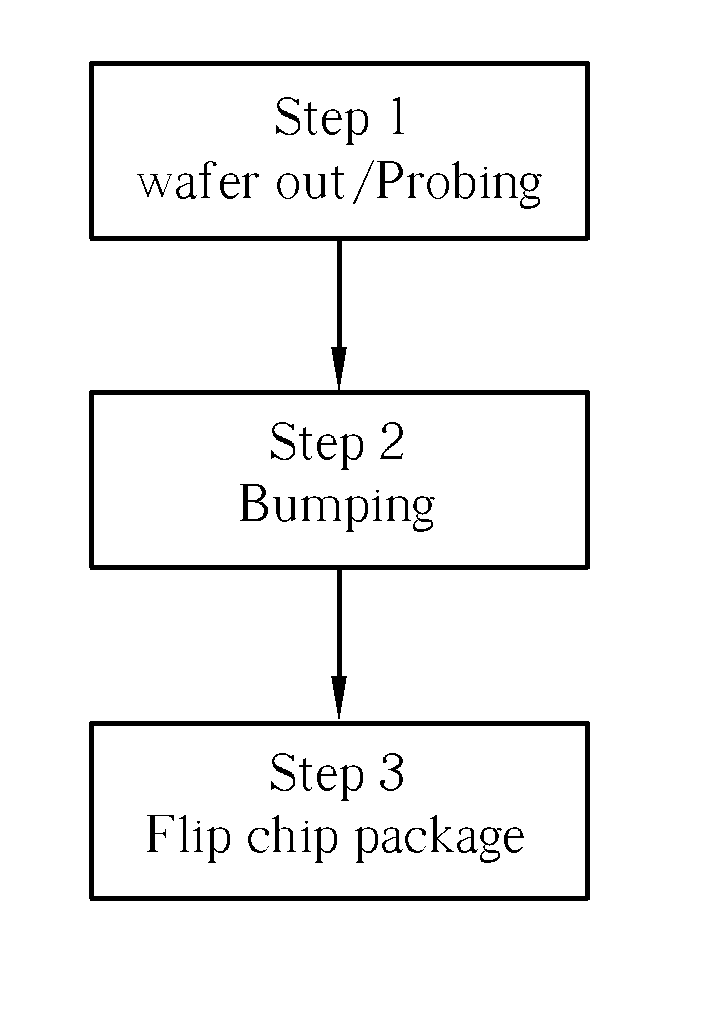
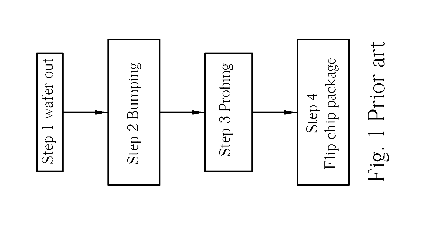
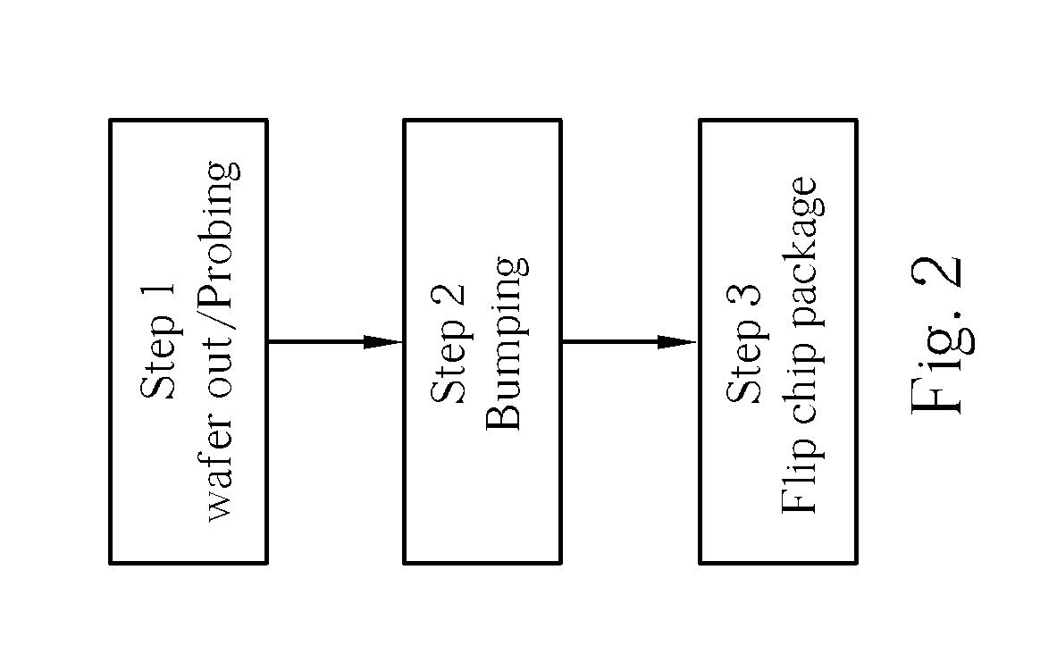
[0025] Please refer to FIG. 2. FIG. 2 is a flowchart of a novel flip-chip packaging process according to the present invention. As shown in FIG. 2, after finishing the fabrication of semiconductor devices on semiconductor wafers (Step 1), the semiconductor wafers are immediately transferred to a testing house for an electrical probing test. Alternatively, probing of the semiconductor wafers may be done by chipmakers themselves. By doing this, when fabrication processes of this batch of wafers went wrong, the yield feedback information will be known immediately. After that, the semiconductor wafers are transferred to a subcontractor for bumping (Step 2). Likewise, this bumping process usually takes 5 to 7 days. After bumping, the wafers are then transferred to a package house in which microchips are placed face down on a substrate such as a printed circuit board that has been prepared with corresponding pads. When heat is applied, the solder re-flows to the pads and the chips are con...


PUM


Abstract

The present invention provides a novel probe tip suited for flip-chip packaging process. The probe tip comprises a needle body; and a stop cylinder having a recess for fittingly accommodating the needle body therein, the needle body being electrically connected to the stop cylinder via a resilient conductive material. The stop cylinder has an annual flat bottom surrounding the needle body for pressing a protruding probe mark on a metal pad scratched by the needle body.

Description

CROSS REFERENCE TO RELATED APPLICATIONS [0001] This is a division application of U.S. patent application Ser. No. 10 / 604,611 filed Aug. 5, 2003 by Liu et al.BACKGROUND OF INVENTION [0002] 1. Field of the Invention [0003] The present invention relates generally to flip-chip packaging processes, and more particularly, to a flip-chip packaging process utilizing an improved probe tip design for implementing a probing process. [0004] 2. Description of the Prior Art [0005] For chip-to-carrier interconnection, IBM uses its Controlled Collapse Chip Connection (C4) technology, widely known as Flip-Chip Attach (FCA). C4 and flip-chip provide high I / O density, uniform chip power distribution, superior cooling capability, and high reliability. Originally developed for use with ceramic carriers in connection with the Solid Logic Technology (SLT) introduced by IBM in the early 1960s, C4 is a process that uses 97 / 3% PbSn solder balls with diameters ranging from 100 to 125 microns as a chip-to-carr...

Claims


Application Information

Patent Timeline
28 Jul 2005
Publication
US20050164428A1
IPC
G01R1/067; G01R31/28; H01L23/485
CPC
G01R1/06738; G01R31/2886; H01L24/10; Y10T436/17; H01L2924/01079; H01L2924/14; H01L2924/01078; H01L2224/05022
Inventors
LIU, HUNG-MIN; CHEN, KOW-BAO