Temperature detection method of semiconductor device and power conversion apparatus

a technology of temperature detection and power conversion apparatus, which is applied in the direction of thermometer details, emergency protective circuit arrangements, process and machine control, etc., can solve the problems of switching loss in semiconductor devices, heat damage, and the possibility of exceeding the allowable temperature, so as to reduce the number of man-hours for wiring and miniaturize the power conversion apparatus

Active Publication Date: 2005-09-08
HITACHI IND EQUIP SYST CO LTD
View PDF5 Cites 24 Cited by
  • Summary
  • Abstract
  • Description
  • Claims
  • Application Information

AI Technical Summary

Benefits of technology

[0014] Thus, as described above, the control portion 400 detects the temperature of the power semiconductor devices. And if the detected temperature reaches a predetermined temperature such as 80 degrees C., it shuts off energization of the power semiconductor devices and stops the heat generation of the power semiconductor devices to keep the temperature from rising so as to protect the power semiconductor devices and the power conversion apparatus.
[0039] In this case, the above described temperature detection device can be directly placed on the circuit board on which the power semiconductor device is mounted. Therefore, there is no need to insulate it electrically from the cooling fin on which the power semiconductor device is placed so that man-hours for wiring can be reduced.
[0040] According to the present invention, it is possible to further miniaturize the power conversion apparatus.

Problems solved by technology

In general, there is a switching loss in a semiconductor device.
Therefore, if excessive currents pass and cooling capacity cannot follow, temperature rises due to the heat generation so that, if left as-is, there is a possibility of exceeding allowable temperature and being destroyed by heat.

Method used


Image

  • Temperature detection method of semiconductor device and power conversion apparatus
  • Temperature detection method of semiconductor device and power conversion apparatus
  • Temperature detection method of semiconductor device and power conversion apparatus

Examples


Embodiment Construction

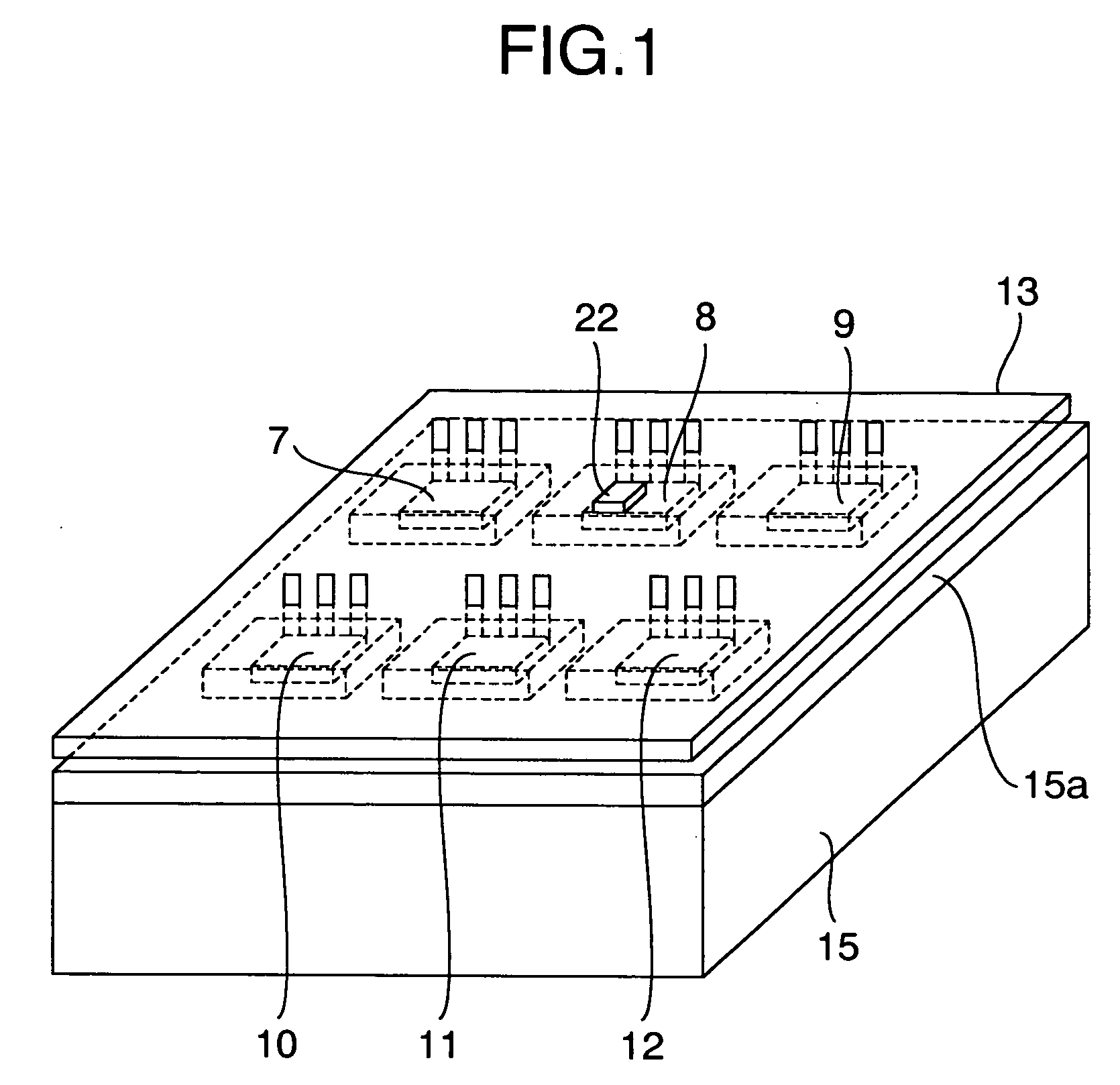
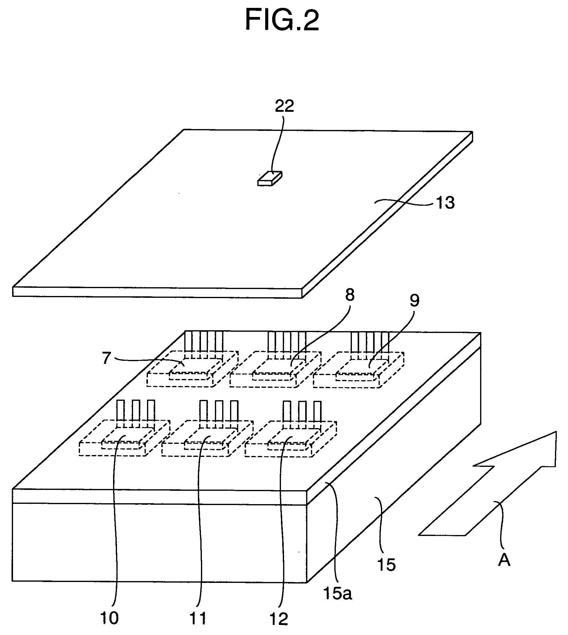
[0053] Hereunder, a detailed description will be given by referring to embodiments shown in the drawings as to a temperature detection method of a semiconductor device and a power conversion apparatus having a function of temperature detection according to the present invention.

[0054]FIG. 1 shows an embodiment of the present invention. In FIG. 1, reference numeral 22 denotes a temperature detection device, and other components are the same as those of the technology described in FIG. 7 wherein components 7 to 12 consisting of packages of power semiconductor devices 1 to 6 are placed on a cooling fin 15 and a circuit board 13 is mounted thereon. FIG. 9 is a sectional view of FIG. 1, and represents a section passing through the components 8 and 11. The components 7 to 12 are put on the cooling fin 15 and are fixed thereon with a plastic case 15a. The circuit board 13 is mounted on topside thereof, and terminals of the components 7 to 12 are soldered thereon. A temperature detection d...


PUM

PropertyMeasurementUnit
distanceaaaaaaaaaa
distanceaaaaaaaaaa
temperatureaaaaaaaaaa

Abstract

There is provided a temperature detection method of a semiconductor device that is small and low-cost and a power conversion apparatus that is small and low-cost. Temperature detection for thermal protection of a power semiconductor device is performed by a temperature detection device placed in the proximity to a component having the power semiconductor device packaged therein and in the proximity to one of an emitter terminal and a collector terminal of the power semiconductor device. As the temperature detection device can be mounted on a circuit board, it is not necessary to insulate the temperature detection device electrically from a cooling fin on which the power semiconductor device is placed and there is no need for lead wires and man-hours for wiring the lead wires. Therefore, it is possible to inexpensively realize the thermal protection of the power semiconductor device in the power conversion apparatus. It is also possible to realize miniaturization of the power conversion apparatus and reduction in assembly time.

Description

BACKGROUND OF THE INVENTION [0001] The present invention relates to a temperature detection technology of a semiconductor device, and in particular, to a temperature detection method of the semiconductor device used for a power conversion apparatus. PRIOR ART [0002] The temperature detection technology of the semiconductor device is described in patent documents 1, 2 and 3. [0003] [Patent Document 1] JP-A-2002-101668 [0004] [Patent Document 2] JP-A-11-142254 [0005] [Patent Document 3] JP-A-2002-76236 BRIEF SUMMARY OF THE INVENTION [0006] In general, there is a switching loss in a semiconductor device. For this reason, a power semiconductor device (semiconductor device for electric power) used for a power conversion apparatus such as an inverter involves considerable heat generation. Therefore, if excessive currents pass and cooling capacity cannot follow, temperature rises due to the heat generation so that, if left as-is, there is a possibility of exceeding allowable temperature an...

Claims


Application Information

Patent Timeline
Patent Type & Authority Applications(United States)
IPC IPC(8): H01L23/34G01K7/01G01K7/22G01K11/00H01L25/04H01L25/07H01L25/11H01L25/18H02M7/00H05K1/02H05K3/34
CPCG01K7/22H01L25/115H02M7/003H05K1/0201H05K3/3447H05K2201/10151H01L2924/0002H05K2201/10166H05K2201/10545H05K2203/304H01L2924/00
Inventor KAMEZAWA, TOMOYATAKATA, NAOKIHIROTA, MASAYUKIHIRAGA, MASAHIROIBORI, SATOSHI
Owner HITACHI IND EQUIP SYST CO LTD
Why Eureka
Try Eureka