Frequency modulator, frequency modulating method, and wireless circuit
Inactive Publication Date: 2005-09-29
PANASONIC CORP
View PDF6 Cites 13 Cited by
Summary
Abstract
Description
Claims
Application Information
AI Technical Summary
This helps you quickly interpret patents by identifying the three key elements:
Problems solved by technology
Method used
Benefits of technology
Benefits of technology
[0015] In this case, the voltage controlled oscillator may include a frequency control terminal connected to the loop filter and a frequency modulation terminal for inputting the control signal, and the voltage controlled oscillator may control the oscillation frequency based on an output of the loop filter and the control signal inputted from the frequency modulation terminal. As a result, it is possible to perform frequency modulation over a wide range of frequencies based on the digital modulation data by using the voltage controlled oscillator having the frequency modulation terminal. Furthermore, the voltage controlled oscillator whose change of output frequency in response to a change in input frequency at the frequency modulation terminal may be smaller compared to its change of output frequency in response to a change in input frequency at the frequency control terminal, thereby enabling to increase the modulation accuracy.
[0026] A fourth aspect of the present invention is directed to a frequency modulator that performs frequency modulation based on digital modulation data, including: a sigma-delta modulator for sigma-delta modulating data obtained by adding a fractional part of provided reference frequency division factor data with modulation data; a reference frequency divider for dividing a frequency of a provided reference signal based on data obtained by adding an output of the sigma-delta modulator with an integral part of the reference frequency division factor data; a voltage controlled oscillator that can control an oscillation frequency; a frequency divider for dividing a frequency of an output of the voltage controlled oscillator; a phase comparator for comparing phases of the reference signal frequency-divided by the reference frequency divider and an output of the frequency divider; and a loop filter for smoothing an output of the phase comparator and providing the smoothed signal to the voltage controlled oscillator, wherein the output of the voltage controlled oscillator is frequency-modulated based on a control signal that is an analog signal converted from data obtained by adding the output of the sigma-delta modulator with the integral part of the reference frequency division factor data. According to the above-described fourth aspect, the same effect can be produced as in the case of the third aspect.
Thus, a PLL does not allow its loop bandwidth to be sufficiently widened.
On the other hand, the above-described second method makes it difficult to modulate over a frequency lower than the PLL loop bandwidth.
However, the narrowed loop bandwidth generally slows the loop response speed of the PLL.
Thus, a PLL does not also allow its loop bandwidth to be sufficiently narrowed.
However, the frequency modulator using the above-described third method has to be supplied with an analog modulation signal, which results in the need of a high-precision D / A converter that converts digital modulation data into the analog modulation signal.
Method used
Image
Click on the blue label to locate the original text in one second.
Reading with bidirectional positioning of images and text.
Examples
first embodiment
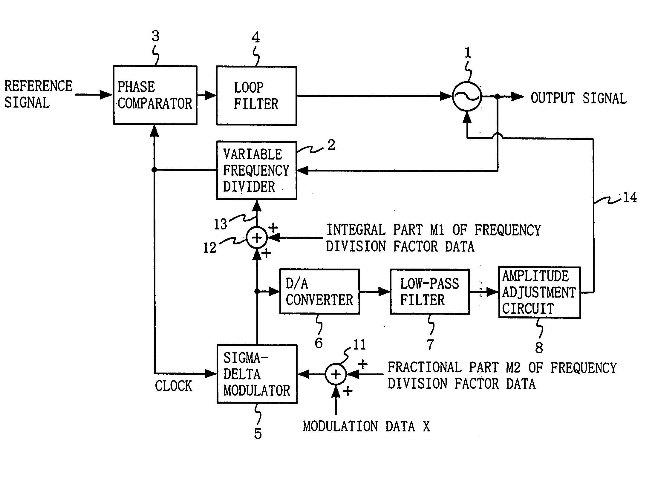
[0048]FIG. 1 is a block diagram illustrating the structure of a frequency modulator according to a first embodiment of the present invention. The frequency modulator shown in FIG. 1 includes a voltage controlled oscillator 1, a variable frequency divider 2, a phase comparator 3, a loop filter 4, a sigma-delta modulator 5, a D / A converter 6, a low-pass filter 7, an amplitude adjustment circuit 8, and adders 11 and 12. A reference signal with a predetermined frequency is provided to the frequency modulator from an external source (not shown), which can be a signal source having no frequency modulation function.
[0049] The voltage controlled oscillator 1, the variable frequency divider 2, the phase comparator 3, and the loop filter 4 form a phase locked loop (PLL) described below. The variable frequency divider 2 divides a frequency of an output signal of the voltage controlled oscillator 1 based on provided effective frequency division factor data 13. The phase comparator 3 compares t...
second embodiment
[0074]FIG. 9 is a block diagram illustrating the structure of the frequency modulator according to a second embodiment of the present invention. The frequency modulator shown in FIG. 9 includes the voltage controlled oscillator 1, the variable frequency divider 2, the phase comparator 3, the loop filter 4, the sigma-delta modulator 5, the D / A converter 6, the low-pass filter 7, the amplitude adjustment circuit 8, a reference frequency divider 9, and the adders 11 and 12. Any components that function in similar manners to their counterparts in the first embodiment are denoted by like numerals, with the descriptions thereof omitted.
[0075] As is the case with the first embodiment, a reference signal with a predetermined frequency is provided to the frequency modulator shown in FIG. 9 from an external signal source (not shown), which can be a signal source having no frequency modulation function. The voltage controlled oscillator 1, the variable frequency divider 2, the phase comparato...
third embodiment
[0081]FIG. 12 is a block diagram illustrating the structure of a wireless circuit according to a third embodiment of the present invention. The wireless circuit according to the present embodiment uses the frequency modulator according to the first or second embodiment. The wireless circuit shown in FIG. 12 includes a reference oscillator 201, a frequency modulator 202, a transmission amplifier 203, a receiving circuit 204, a duplexer 205, and an antenna 206. This wireless circuit transmits and receives data to and from a wireless circuit at the other end (not shown).
[0082] The reference oscillator 201 generates a reference signal with a predetermined frequency. The reference oscillator 201 is structured by, for example, a crystal oscillator whose operation is stable. The reference signal generated by the reference oscillator 201 is provided to the frequency modulator 202. The frequency modulator 202 is a frequency modulator according to the first or second embodiment, and operates...
PUM
Abstract
A voltage controlled oscillator 1, a variable frequency divider 2, a phase comparator 3, and a loop filter 4 form a Phase Locked Loop (PLL). A sigma-delta modulator 5 sigma-delta modulates data obtained by adding a fractional part M2 of the frequency division factor data with modulation data X by using an output signal of the variable frequency divider 2 as a clock. An output signal of the sigma-delta modulator 5 is added to an integral part M1 of the frequency division factor data, and the resultant data becomes effective frequency division factor data 13 of the variable frequency divider 2. An output signal of the sigma-delta modulator 5 also becomes control data 14 after passing through a D / A converter 6, a low-pass filter 7, and an amplitude adjustment circuit 8. The control data 14 is inputted into a frequency modulation terminal of the voltage controlled oscillator 1. Therefore, it is possible to provide a frequency modulator that can use a reference signal source having no frequency modulation function, and perform modulation over a wide range of frequencies based on a digital modulation signal.
Description
BACKGROUND OF THE INVENTION [0001] 1. Field of the Invention [0002] The present invention relates to frequency modulators, more particularly, a frequency modulator and a frequency modulating method for performing frequency modulation using a PLL (Phase Locked Loop), and a wireless circuit using the frequency modulator and the frequency modulating method. [0003] 2. Description of the Background Art [0004] As exemplary methods for performing frequency modulation using a PLL, the following two methods are known. In a first method, a reference signal source is subjected to frequency modulation. In a second method, a modulation signal is supplied to a frequency control terminal of a voltage controlled oscillator. In general, the modulation signal used in digital communications, etc., has flat frequency characteristics from low to high frequencies within a predetermined band. Thus, in the case where frequency modulation is performed based on such a modulation signal, flat characteristics ...
Claims
Application Information
Patent Timeline
Application Date:The date an application was filed.
Publication Date:The date a patent or application was officially published.
First Publication Date:The earliest publication date of a patent with the same application number.
Issue Date:Publication date of the patent grant document.
PCT Entry Date:The Entry date of PCT National Phase.
Estimated Expiry Date:The statutory expiry date of a patent right according to the Patent Law, and it is the longest term of protection that the patent right can achieve without the termination of the patent right due to other reasons(Term extension factor has been taken into account ).
Invalid Date:Actual expiry date is based on effective date or publication date of legal transaction data of invalid patent.

