

Electronic circuit with embedded memory
a technology of embedded memory and electronic circuits, applied in the field of circuitry, can solve the problems of large chip area consumed by laterally oriented devices, large amount of chip area consumed by processor circuits, and large amount of idle processor circuits
- Summary
- Abstract
- Description
- Claims
- Application Information
AI Technical Summary
Benefits of technology
Problems solved by technology
Method used
Image

Examples
Embodiment Construction
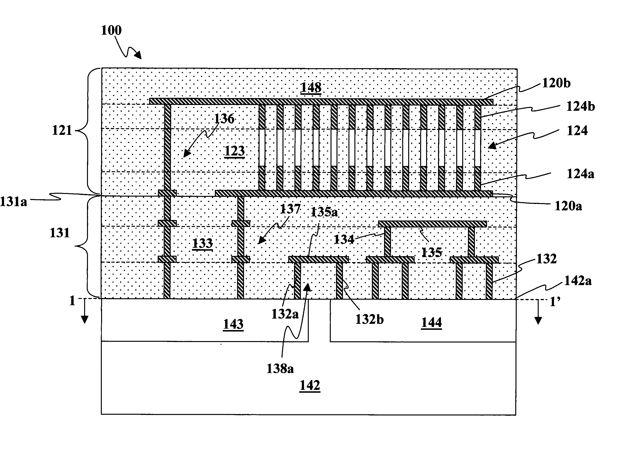
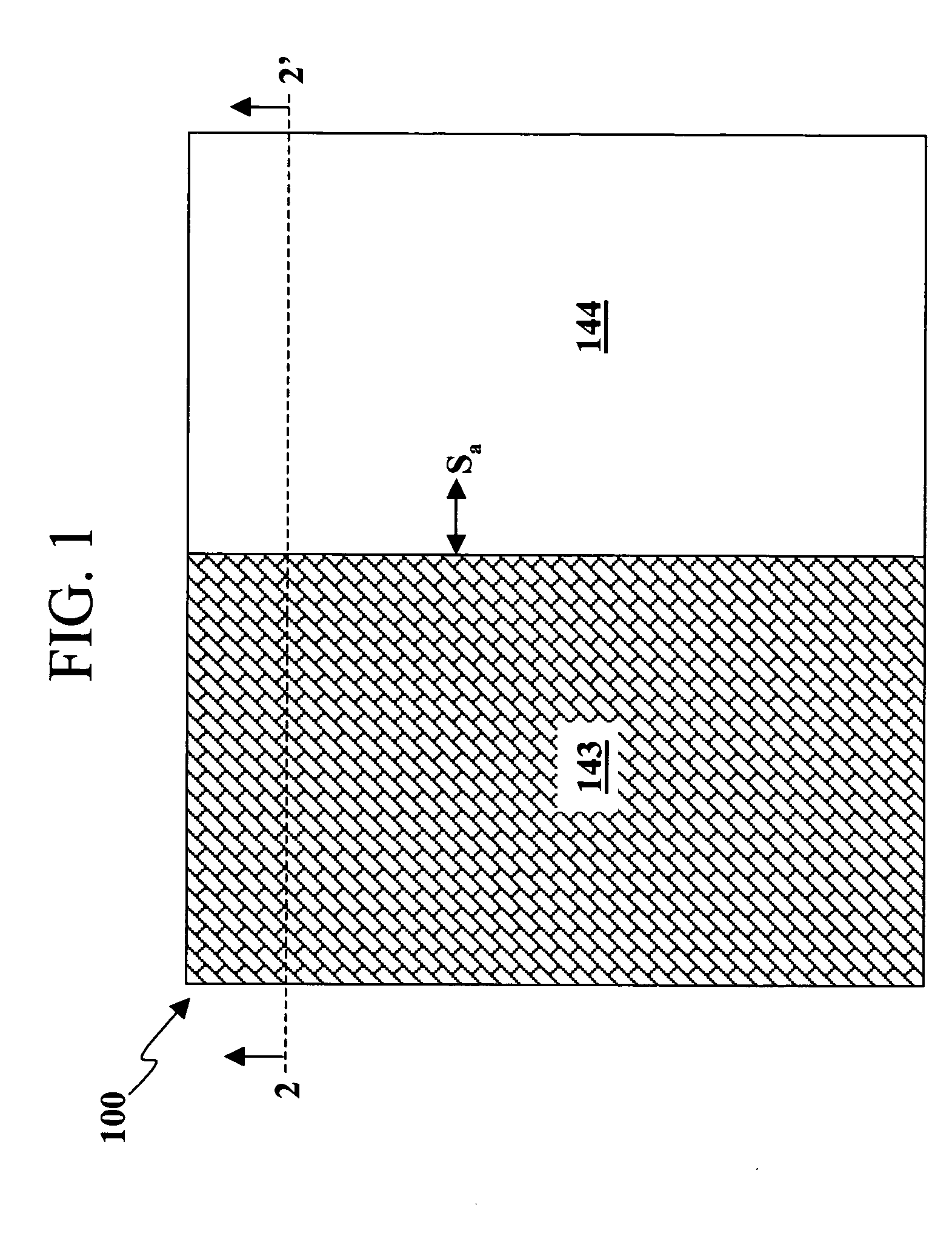
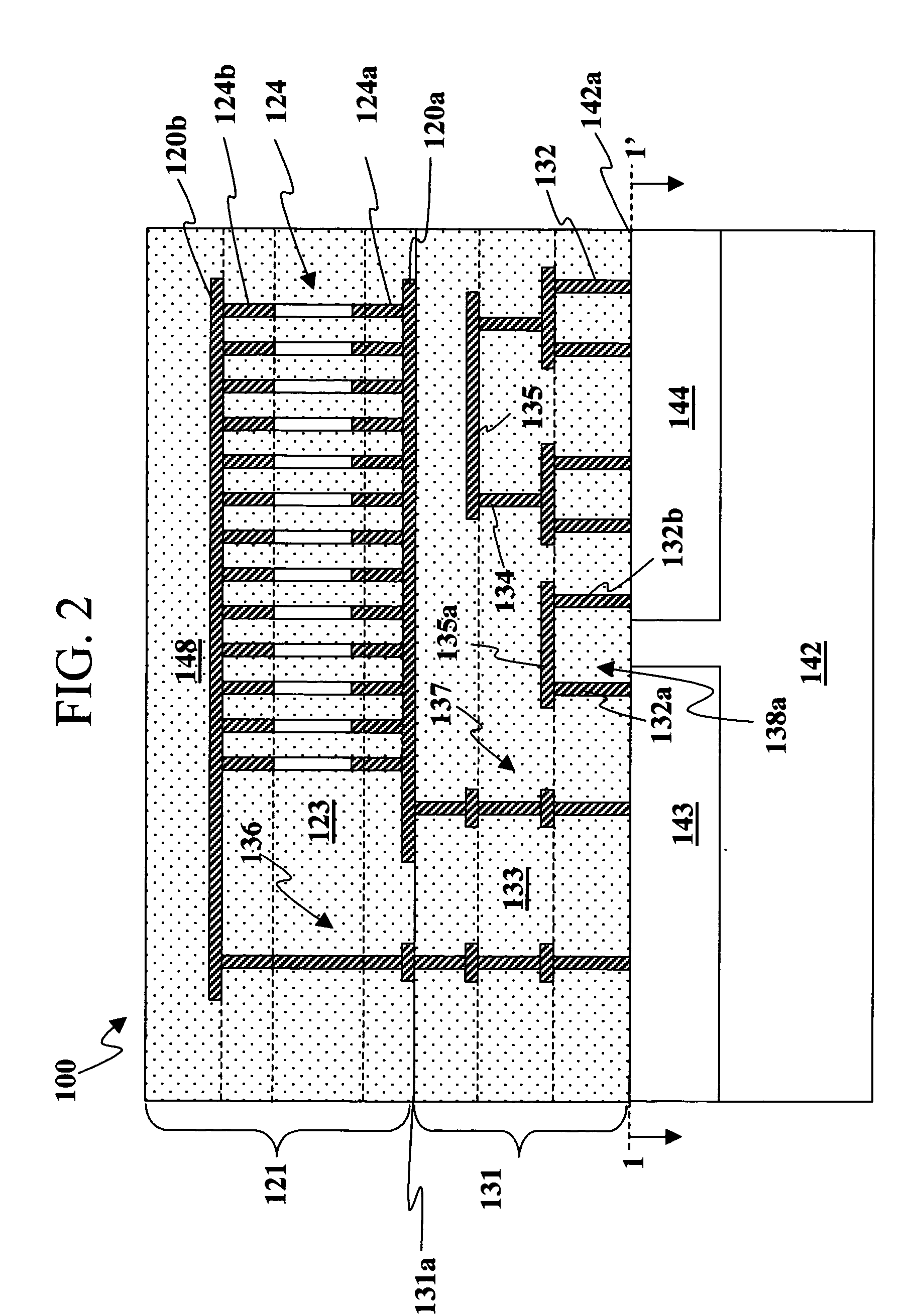
[0033]FIGS. 1 and 2 show simplified top and cross sectional views of a computer chip 100 which includes circuitry, in accordance with the present invention. FIG. 1 is a top view taken along a cut-line 1-1′ of FIG. 2 and FIG. 2 is a sectional view taken along a cut-line 2-2′ of FIG. 1. It should be noted that in the following figures, like reference characters indicate corresponding elements throughout the several views.
[0034] In this embodiment, computer chip 100 includes processor and control circuits which are carried by a substrate and coupled together so that signals can flow between them. Computer chip 100 also includes a memory circuit positioned above the processor and control circuits. The memory circuit is spaced apart from the processor and control circuits by an interconnect region. The memory circuit is also coupled to the control circuit through the interconnect region so that signals can flow therebetween. In this way, the control circuit can receive output signals fr...
PUM
| Property | Measurement | Unit |
|---|---|---|
| access time | aaaaa | aaaaa |
| size | aaaaa | aaaaa |
| size | aaaaa | aaaaa |
Abstract
Description
Claims
Application Information