
Optimized reference voltage generation using switched capacitor scaling for data converters

a data converter and switched capacitor technology, applied in the field of semiconductor circuits, can solve problems such as mismatching the scaling between the reference generator and the interface function, and the requirements are often contradictory to each other, and achieve the effect of improving the scaling efficiency and reducing the cos

Inactive Publication Date: 2005-10-06
NORTH STAR INNOVATIONS
View PDF12 Cites 56 Cited by
  • Summary
  • Abstract
  • Description
  • Claims
  • Application Information

AI Technical Summary

Problems solved by technology

These requirements are often contradictory to one another.
Furthermore, cost is an important factor that directly correlates to the amount of semiconductor area needed to implement a design.
Such circuits introduce a number of problems that result in a mis-match in scaling between the reference generator and the interface function.
This mis-match, between the two scaling functions results in either an A / D converter transfer gain error, transfer offset error or both.
Additionally, the scaled output voltages require large capacitors that are typically required to be implemented external to an integrated circuit chip due to their required size.
As a result, the generation of scaled reference voltages for use in an RSD data converter introduces error, requires additional circuitry and package support pins.

Method used


Image

  • Optimized reference voltage generation using switched capacitor scaling for data converters
  • Optimized reference voltage generation using switched capacitor scaling for data converters
  • Optimized reference voltage generation using switched capacitor scaling for data converters

Examples


Embodiment Construction

[0021] The following detailed description is merely exemplary in nature and is not intended to limit the invention or the application and uses of the invention. Furthermore, there is no intention to be bound by any expressed or implied theory presented in the preceding technical field, background, brief summary or the following detailed description.

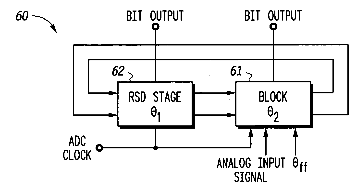
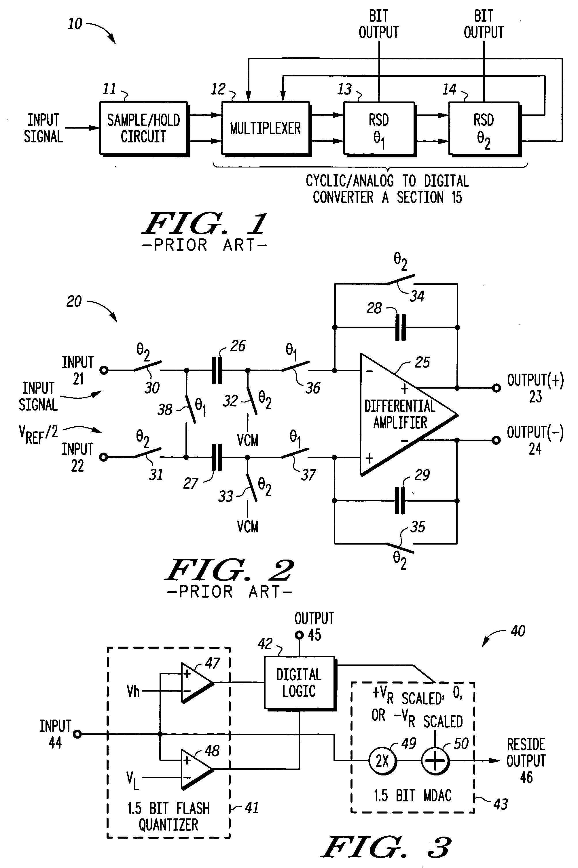
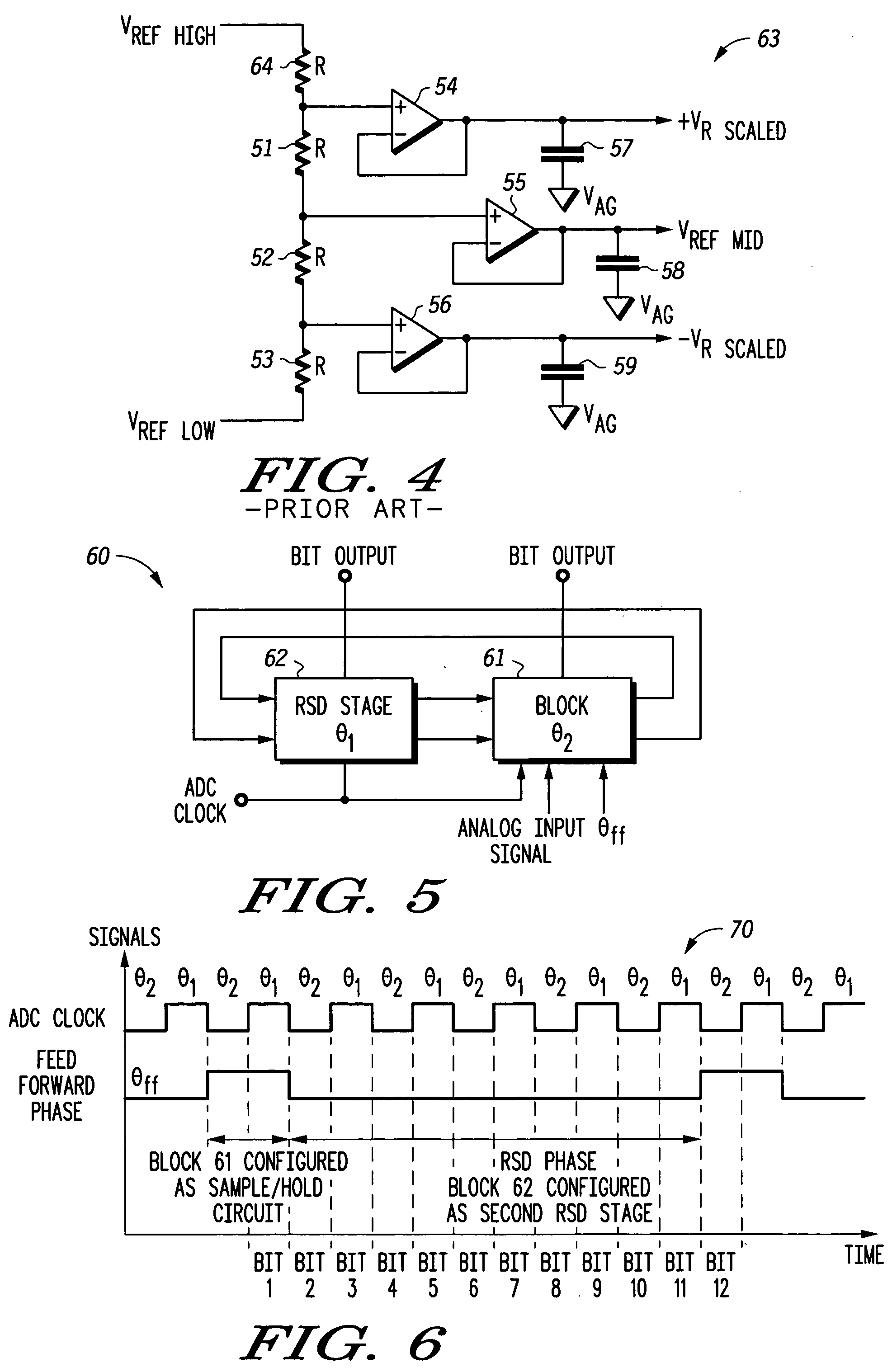
[0022]FIG. 1 is a block diagram of a prior art redundant signed digit (RSD) cyclical analog to digital converter 10 having two RSD stages. In general, RSD cyclical analog to digital converter 10 is a clocked system that samples an analog voltage and generates an N-bit digital word representing the sampled analog voltage, where N is an integer. The number of bits (N) of the digital word corresponds to the resolution of the conversion process and is chosen based on the application requirements. Typically, the complexity, size, and power of the converter increase with speed of conversion and resolution.

[0023] While FIG. 1 illustrates an RS...


PUM


Abstract

An algorithmic or cyclic data converter uses an RSD stage having a switched capacitor network for efficiently scaling at least one externally supplied reference voltage. A reference voltage is scaled by using capacitor ratios that also function to provide an output voltage used as a residue output of the RSD A / D converter. The residue is used to generate a bit value corresponding to the magnitude of the residue. Two RSD stages cycle back and forth generating a logic value each half clock cycle until the desired bit resolution is achieved. In one form, the RSD stage scales the externally supplied reference voltage only by factors of less than one. In another form, the RSD stage scales the reference voltage by any scaling factor. A reference voltage scaling circuit separate from the RSD stage is avoided.

Description

RELATED APPLICATION [0001] This application is related to: [0002] U.S. patent application Ser. No. 10 / 631,450, entitled “Space Efficient Low Power Cyclic A / D Converter” filed Jul. 30, 2003, and assigned to the assignee hereof.TECHNICAL FIELD OF INVENTION [0003] The present invention generally relates to semiconductor circuits, and more particularly relates to data conversion. BACKGROUND OF INVENTION [0004] Digital signal processing has been proven to be very efficient in handling and manipulating large quantities of data. There are many products that are in common use such as wireless devices, digital cameras, motor controllers, automobiles, and toys, to name a few, that rely on digital signal processing to operate. Many of these products continuously receive information that is monitored and used to produce adjustments to the system thereby maintaining optimum performance. The data is often an analog signal that must be converted to a representative digital signal. For example, lig...

Claims


Application Information

Patent Timeline
Patent Type & Authority Applications(United States)
IPC IPC(8): H03M1/12H03M1/16H03M1/66
CPCH03M1/162
Inventor ATRISS, AHMAD H.ALLEN, STEVEN P.GARRITY, DOUGLAS A.
Owner NORTH STAR INNOVATIONS
Learn More