Liquid crystal display device
a liquid crystal display and display device technology, applied in non-linear optics, instruments, optics, etc., can solve the problems of deterioration of luminance, lack of research on improving the picture quality of lcd devices, and uniformity of lcd devices, so as to maximize the luminance of lcd devices
- Summary
- Abstract
- Description
- Claims
- Application Information
AI Technical Summary
Benefits of technology
Problems solved by technology
Method used
Image
Examples
first embodiment
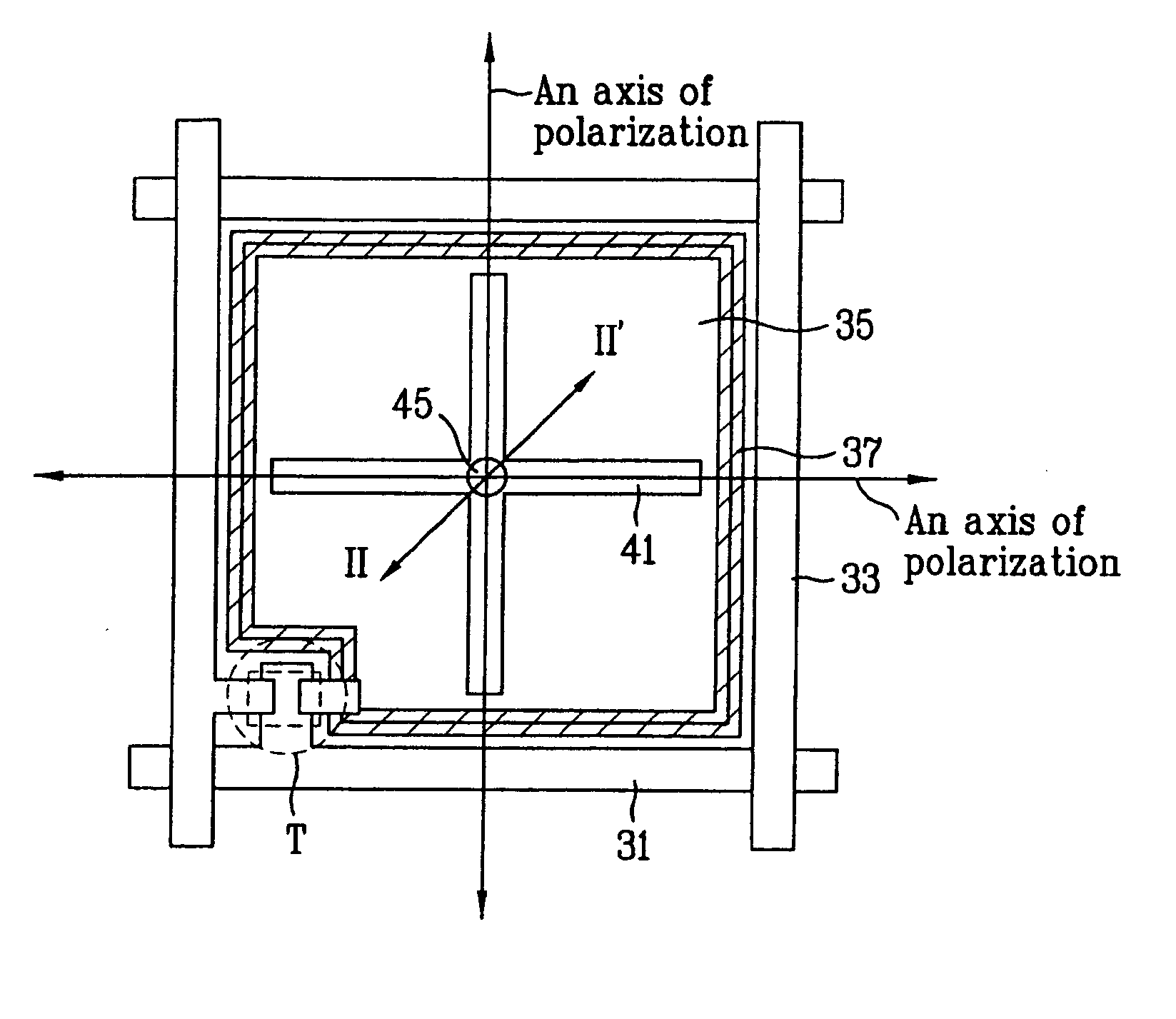
[0050] As illustrated in FIG. 6 and FIG. 7, the LCD device according to the present invention includes lower and upper substrates 30 and 40 facing each other with a predetermined interval therebetween. A plurality of gate and data lines 31 and 33, a plurality of thin film transistors T, a pixel electrode 35, a common auxiliary electrode 37, a gate insulating layer 32, and a passivation layer 34 are on the lower substrate 30. A black matrix layer (not shown), a color filter layer 42, a common electrode 44, a dielectric protrusion 45 are on the upper substrate 40. A liquid crystal layer 46 fills the predetermined interval between the lower and upper substrates 30 and 40.
[0051] The plurality of gate lines 31 are formed on the lower substrate 30 substantially perpendicular to the plurality of data lines 33 for defining a plurality of pixel regions. Then, the plurality of thin film transistors T are formed at crossing points of the plurality of gate and data lines 31 and 33, and each pix...
second embodiment
[0067] In an LCD device according to the present invention, a hole or groove is formed in a pixel region on a color filter layer, and then an electric field inducing window is formed in the center of the hole or groove of the color filter layer.
[0068]FIG. 12 is an enlarged plan view illustrating a unit pixel region of an LCD device according to the second embodiment of the present invention, and FIG. 13 is a cross-sectional view illustrating a unit pixel region taken along line III-III′ of FIG. 10 in an LCD device according to the second embodiment of the present invention.
[0069] As shown in FIG. 12 and FIG. 13, the LCD device according to the second embodiment of the present invention includes lower and upper substrates 30 and 40 facing each and spaced apart by a predetermined interval. The lower substrate 30 includes a plurality of gate and data lines 31 and 33, a plurality of thin film transistors T, a pixel electrode 35, a common auxiliary electrode 37, a gate insulating layer ...
PUM
| Property | Measurement | Unit |
|---|---|---|
| electric field | aaaaa | aaaaa |
| dielectric anisotropy | aaaaa | aaaaa |
| shape | aaaaa | aaaaa |
Abstract
Description
Claims
Application Information


