

Defect identification system and method for repairing killer defects in semiconductor devices
- Summary
- Abstract
- Description
- Claims
- Application Information
AI Technical Summary
Problems solved by technology
Method used
Image

Examples
Embodiment Construction
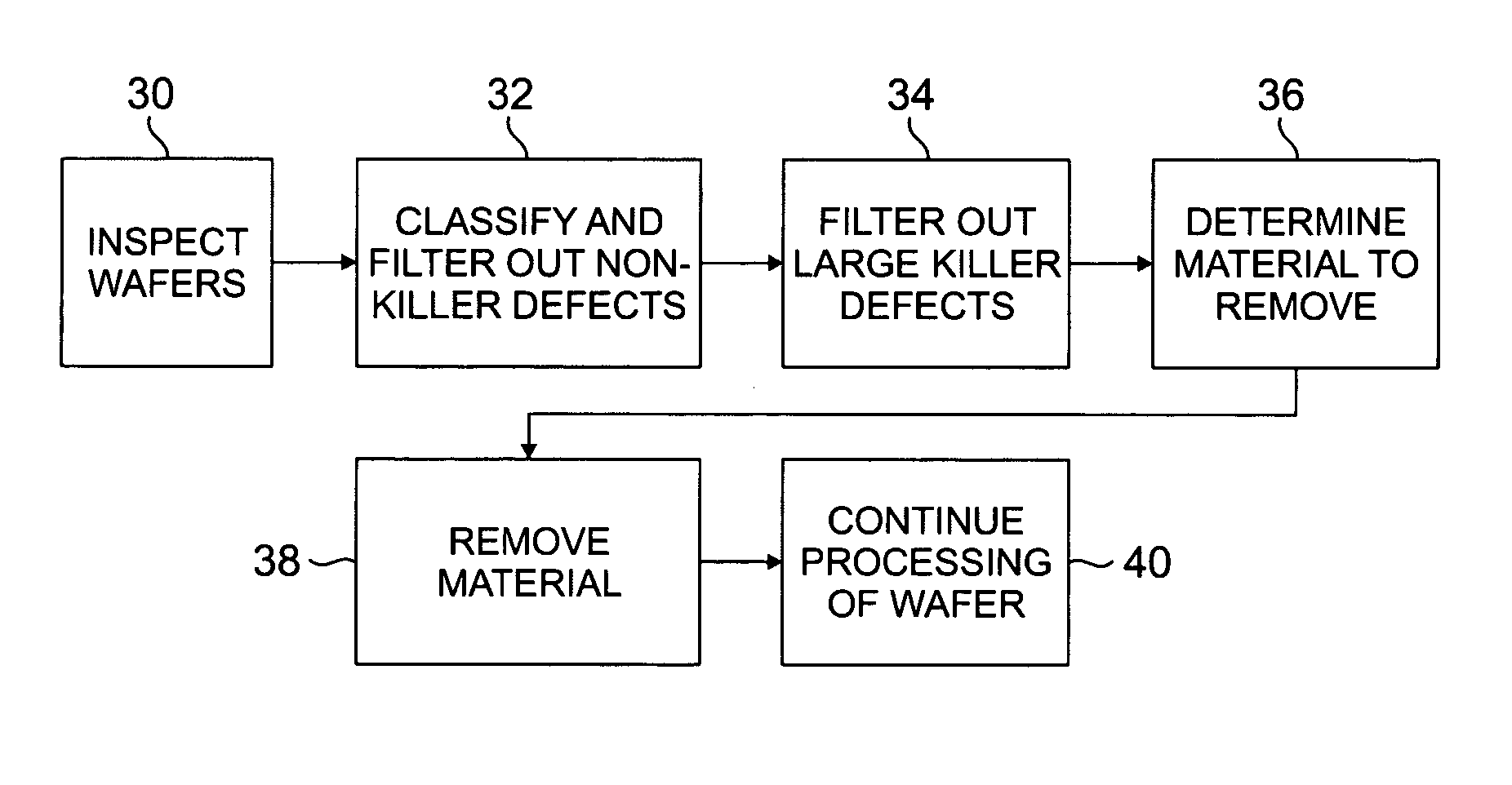
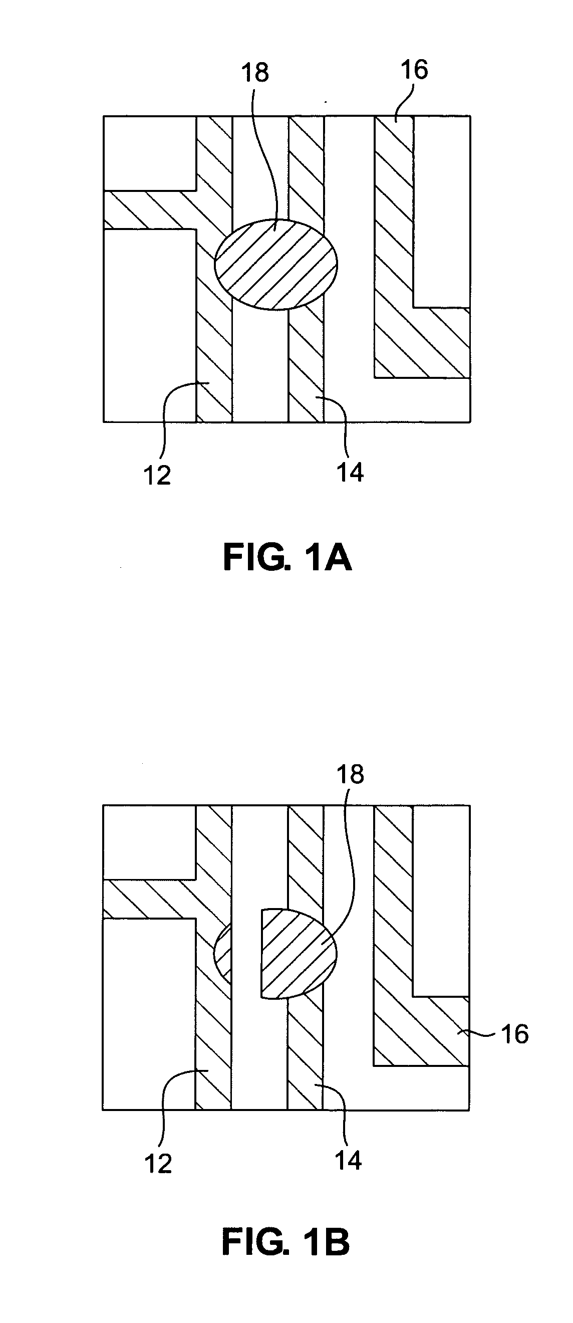
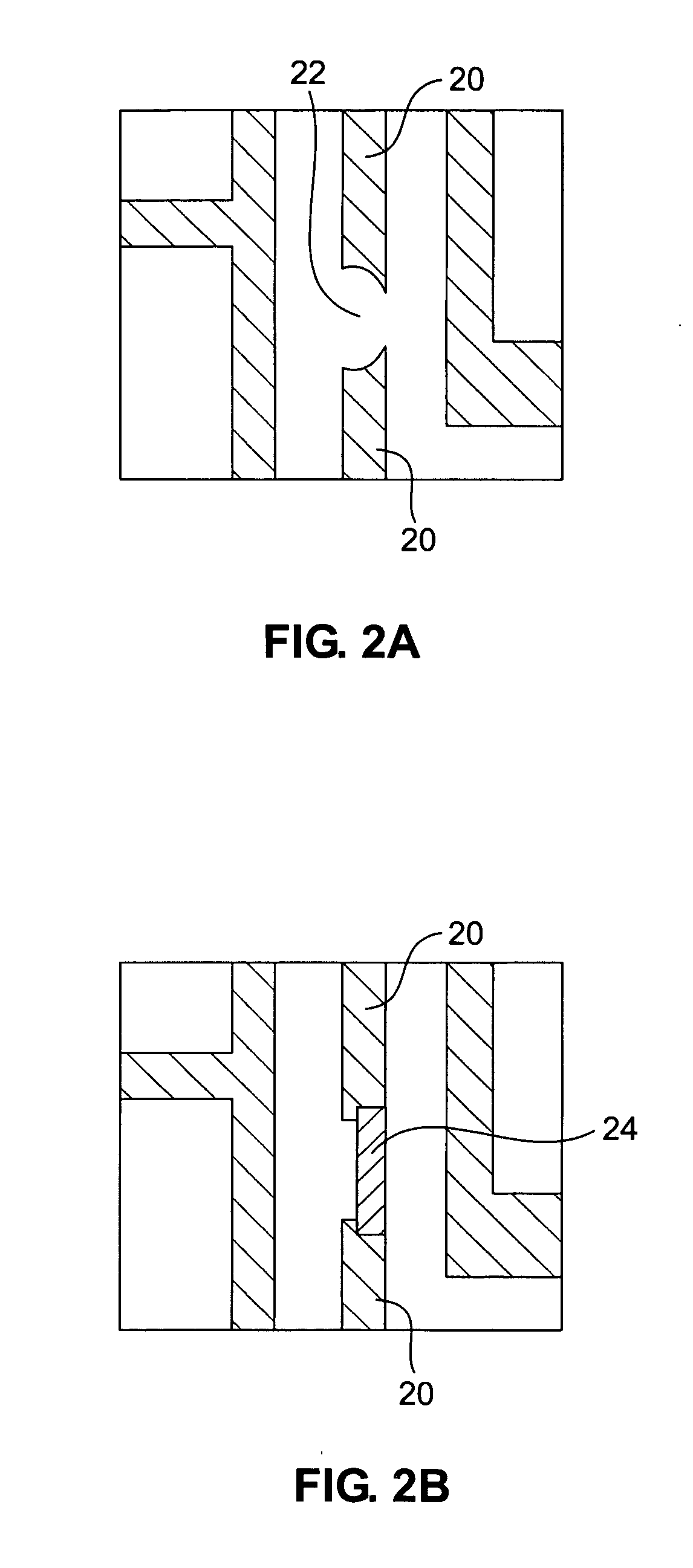
[0011] The majority of the yield lost for integrated circuits is due to defects that are of sub-micron size, short elements of a single mask level (such as metal or gate stack runners) together or create opens at the same levels and can be detected using in-line inspection tools. The shorting mechanisms include metal to metal shorts in either copper or aluminum technologies, gate-stack to gate-stack shorts, gate-stack to window shorts and active region to active region shorts. In-line inspection tools are capable of detecting and locating most of these shorted conditions. For example, U.S. Pat. No. 6,047,083 describes a method and apparatus for pattern inspection that can be used to identify killer defects on semiconductor dies. Most killer defects create a single short between two adjacent elements and therefore only need a minor repair to become non-yield limiting. However, the present invention contemplates that killer defects that cause shorts between more than two elements coul...
PUM
 Abstract
Description
Claims
Application Information