Solid-state image-pickup sensor and device
a solid-state image and sensor technology, applied in the field of solid-state image pick-up sensors, can solve the problems of deteriorating image quality and complex processing required
- Summary
- Abstract
- Description
- Claims
- Application Information
AI Technical Summary
Benefits of technology
Problems solved by technology
Method used
Image
Examples
first embodiment
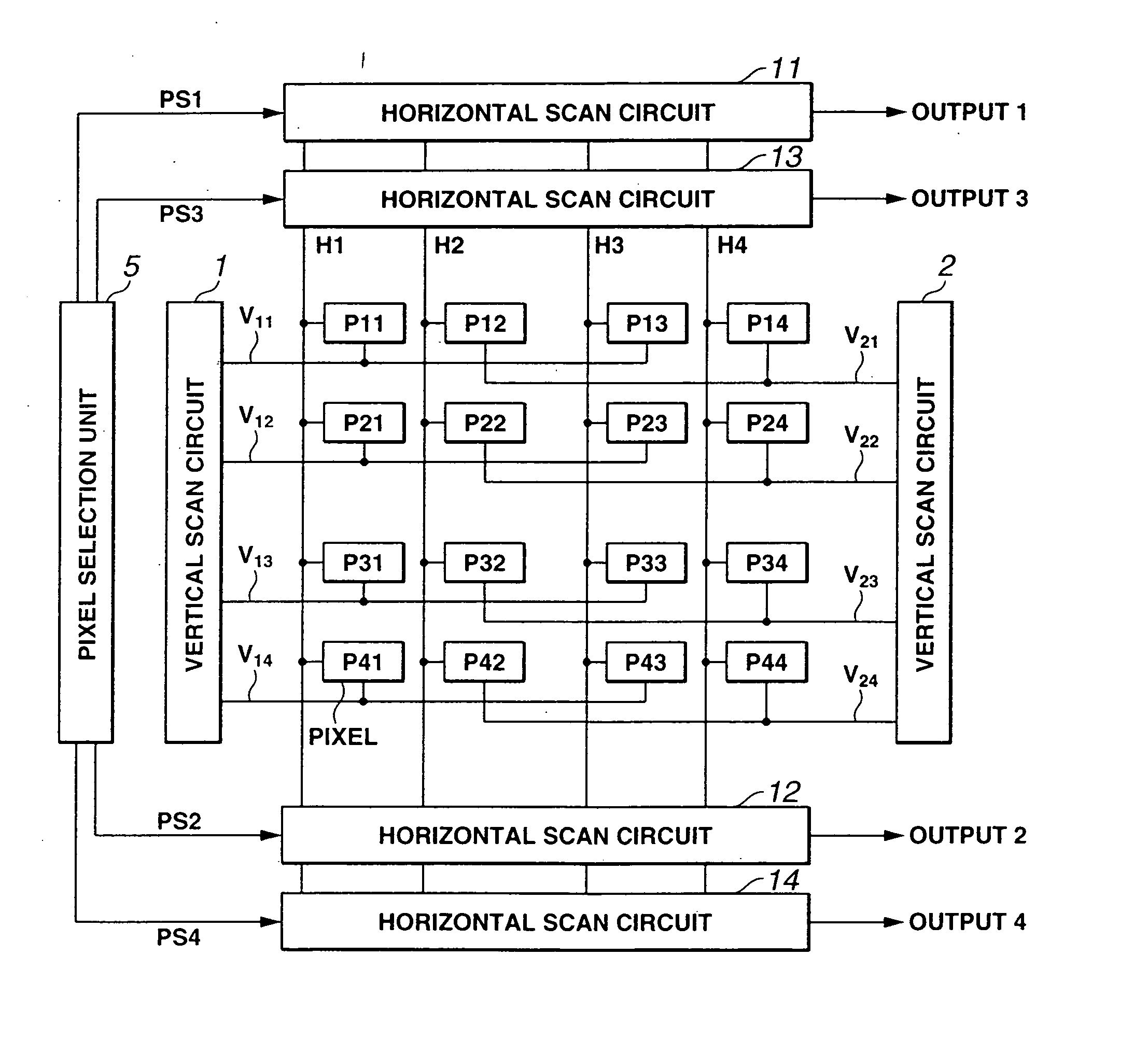
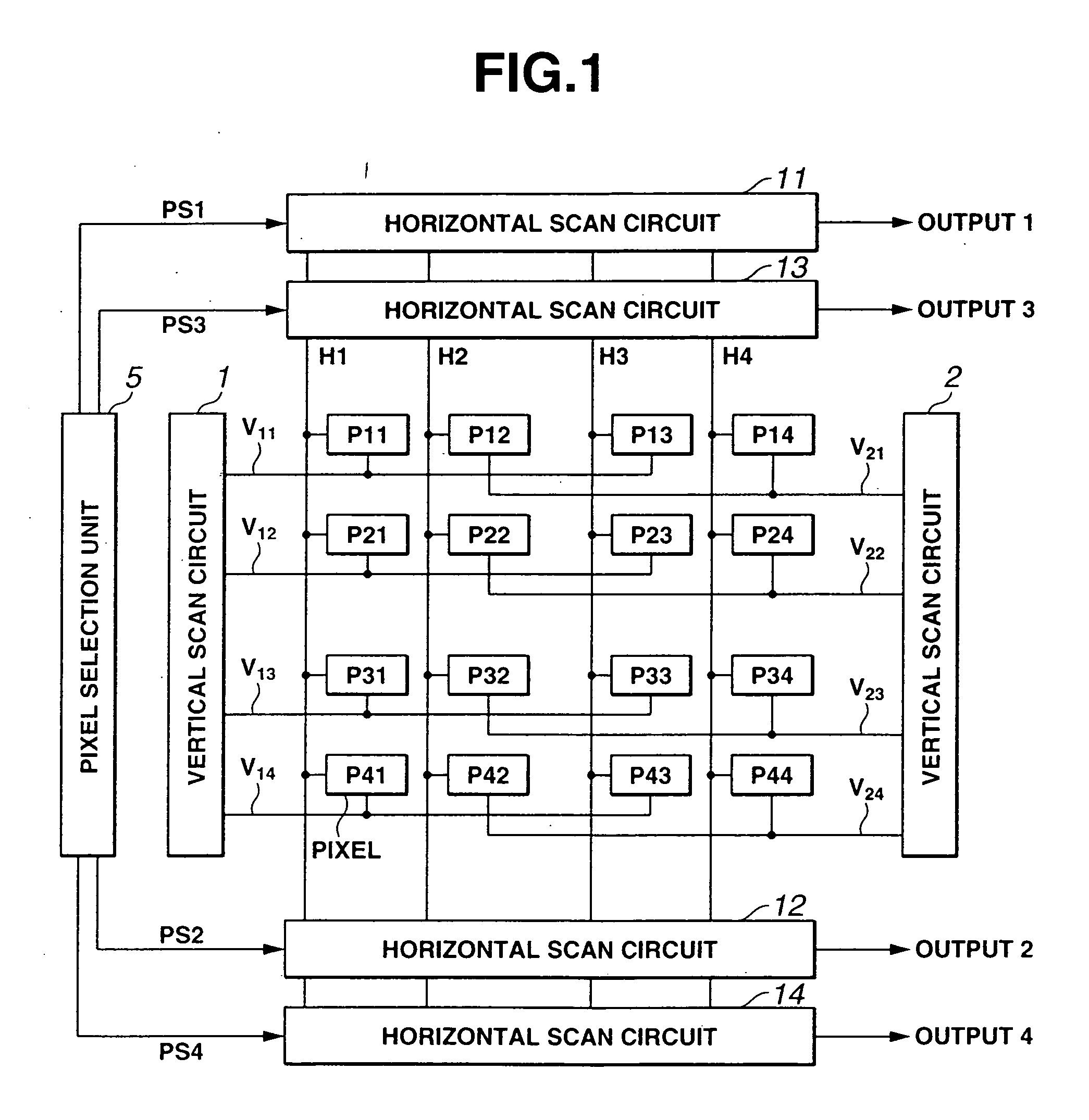
[0032]FIG. 1 is a block diagram of a solid-state image-pickup sensor according to a first embodiment of the present invention. This first embodiment is described in connection with, by way of example, a solid-state image-pickup sensor of X-Y addressing type. In the X-Y addressing type, pixels constructed of photoelectric conversion elements are X-Y addressed to detect charges generated in the conversion elements.
[0033] The solid-state image-pickup sensor shown in the first embodiment of FIG. 1 comprises a plurality (2 in FIG. 1) of vertical scan circuits 1, 2, a plurality (4 in FIG. 1) of horizontal scan circuits 11, 12, 13 and 14, a pixel section including a plurality (16 in FIG. 1) of pixels constructed of respective photoelectric conversion elements arrayed in a matrix, each of which is connected to one of the plurality of vertical scan circuits 1, 2 and connected to the plurality (4 in FIG. 1) of horizontal scan circuits 11, 12, 13 and 14, and a pixel selection unit 5 for contr...
second embodiment
[0052]FIG. 3 is a block diagram of a solid-state image-pickup sensor according to a second embodiment of the present invention. As with the first embodiment, this second embodiment is also described in connection with, by way of example, a solid-state image-pickup sensor of X-Y addressing type.
[0053] The second embodiment has a basic configuration similar to that of the first embodiment except that two more vertical scan circuits are additionally provided. A pixel selection unit is omitted in FIG. 3 for the sake of simplicity in the following description of basic (specific) operation of the solid-state image-pickup sensor shown in FIG. 3.
[0054] Vertical selection lines V11, V12 are extended from one 1A of four vertical scan circuits 1A, 2A, 3A and 4A. The vertical selection line V11 is connected to pixels P11, P13, and the vertical selection line V12 is connected to pixels P31, P33. Vertical selection lines V21, V22 are extended from the vertical scan circuit 2A. The vertical sele...
third embodiment
[0074]FIG. 5 is a configuration figure of pixels and a control unit for the pixels in a solid-state image-pickup sensor according to a third embodiment of the present invention. The block diagram of the solid-state image-pickup sensor according to the third embodiment of the present invention is the same as that shown in FIG. 3, and therefore it is omitted in FIG. 5.
[0075] Because all of the pixels have the same configuration, the following description is made of, by way of example, the pixel P11 for which the read is controlled by the vertical scan circuit 1A shown in FIG. 3. Any of the other pixels also has the same configuration as the pixel P11. The read of the pixel P11 is controlled by the vertical scan circuit 1A together with the pixel P31. Any of the other vertical scan circuits 2A-4A also has the same configuration as the vertical scan circuit 1A.
[0076]FIG. 5 shows a typical one of the pixels and the control unit for the pixels in the form of a simplified diagram, includ...
PUM
 Abstract
Description
Claims
Application Information


