Masking circuit removing unknown bit from cell in scan chain

a scan chain and unknown bit technology, applied in the field of design for testing circuits in integrated circuits, can solve the problems of generating bypass patterns, reducing the efficiency of scan chain,

Active Publication Date: 2014-11-11
TEXAS INSTR INC
View PDF27 Cites 18 Cited by
  • Summary
  • Abstract
  • Description
  • Claims
  • Application Information

AI Technical Summary

Problems solved by technology

These conventional compressors are susceptible to unknowns (Xs) in the circuit.
However, this results in significant loss of compression since the compactor is bypassed in presence of Xs.
Compressed scan chains hitherto have been difficult to use to do debug and result in generation of bypass patterns to isolate the flip-flop that is failing.
In some cases a tool can generate patterns where internal scan chains are observed but this means regeneration of patterns and does neither mean that the same data will be observed, nor guarantee same paths will be excited, and has other problems.
(a) Tasks of debug and diagnostics, wherein the cause of one or more failing outputs in one or more cycles must be diagnosed to one or a set of flip-flops in the design (which in turn drive these outputs), are rendered more difficult. Difficulty arises since (i) the fault localization to the set of failing flip-flops must now be performed with less volume of output data, i.e. reduced observability, and (ii) a given fault may be exercised fewer times as the input decompressor drives few primary scan inputs into a larger number of internal scan inputs, thereby impairing the ability to excite a fault multiple times.
(b) Distinguishing groups of internal scan chains for the purpose of test coverage improvement is rendered more difficult since per cycle individual scan chain observability is no longer possible, on account of multiple internal scan chain outputs being grouped together into fewer primary scan outputs through the output compactor logic.
The latter has inherent disadvantages of (i) requiring a larger number of test cycles and (ii) of introducing a different state of the circuit as compared to that which actually caused a pattern to fail.

Method used


Image

  • Masking circuit removing unknown bit from cell in scan chain
  • Masking circuit removing unknown bit from cell in scan chain
  • Masking circuit removing unknown bit from cell in scan chain

Examples


Embodiment Construction

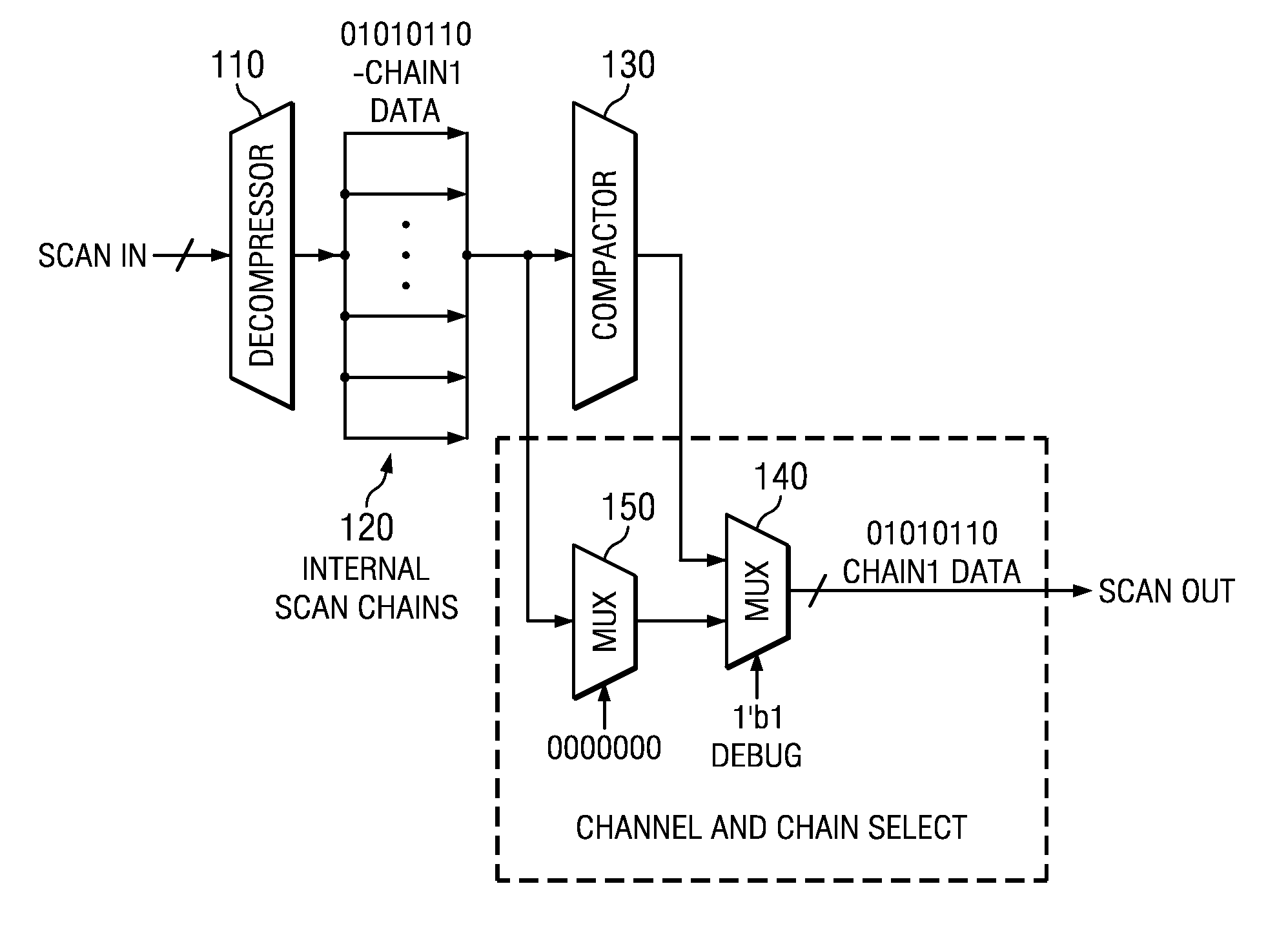
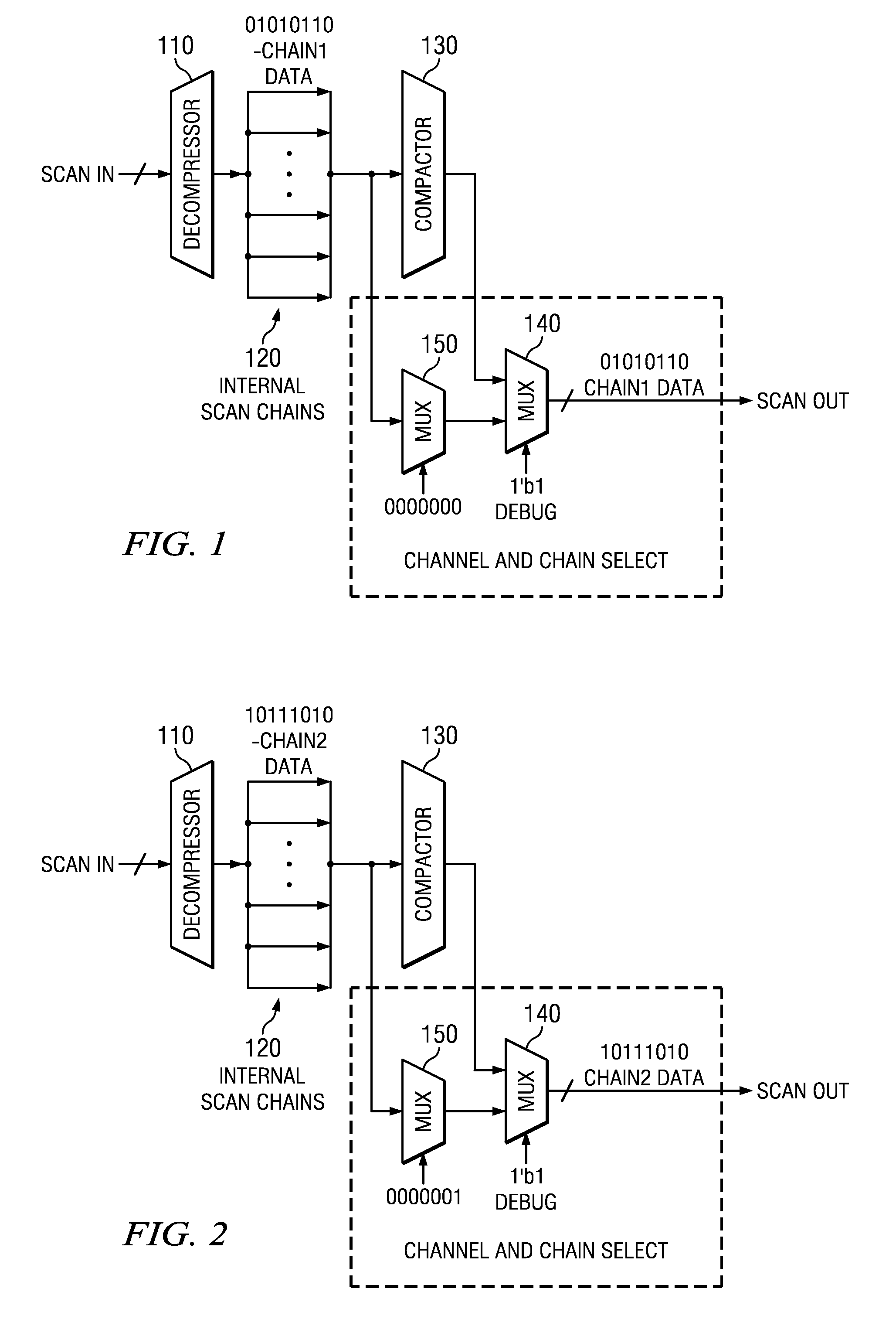
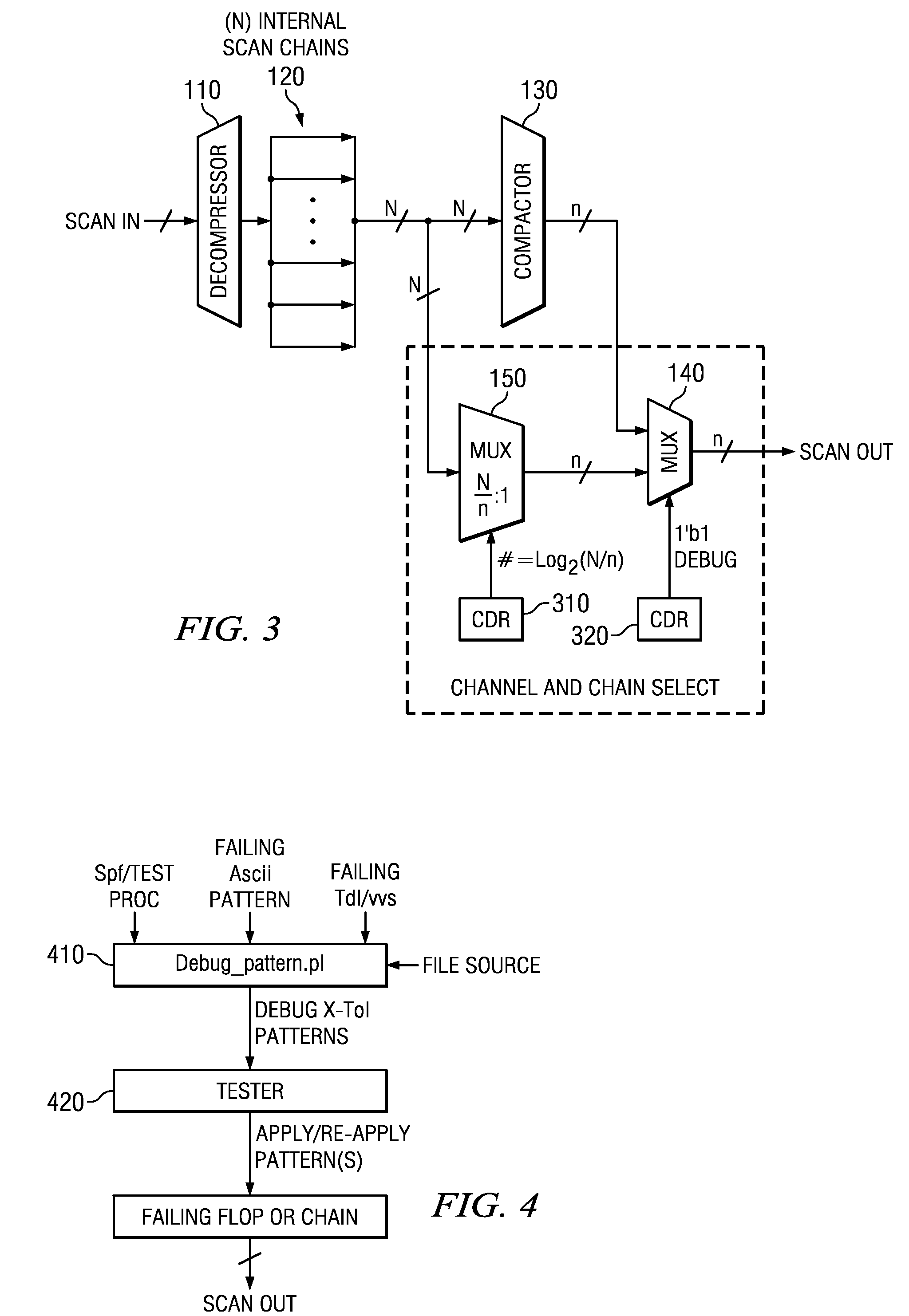
[0038]The inventive embodiments described hereinbelow address and solve the above-mentioned problems discussed in the Background, as well as other problems. They provide selective observability under user control of internal serial channels provided into a functional integrated circuit and that are scan chains called STUMPS. Such selective observability promotes ease of diagnostics as well as fault coverage recovery with reduced test time by including the output compactor for observing the selected set of internal scan chains, e.g. without, in some of the embodiments, resorting to a bypass mode bypassing the compactor.

[0039]This way, selection of a subset of set of scan chains, which are amenable for compaction (and disabling others that have a significant X content that in turn prevents meaningful compaction), is desirably enabled.

[0040]Embodiments of structure and process keep the original pattern set that was developed. By changing the setup / header content of the pattern set / tdl,...


PUM


Abstract

Electronic scan circuitry includes a decompressor (510), a plurality of scan chains (520.i) fed by the decompressor (510), a scan circuit (502, 504) coupled to the plurality of scan chains (520.i) to scan them in and out, a masking circuit (590) fed by the scan chains (520.i), and a scannable masking qualification circuit (550, 560, 580) coupled to the masking circuit (590), the masking qualification circuit (550, 560, 580) scannable by scan-in of bits by the decompressor (510) along with scan-in of the scan chains (520.i), and the scannable masking qualification circuit (550, 560, 580) operable to hold such scanned-in bits upon scan-out of the scan chains through the masking circuit (590). Other scan circuitry, processes, circuits, devices and systems are also disclosed.

Description

CROSS-REFERENCES TO RELATED APPLICATIONS[0001]This application is related to India Patent Application 1625 / CHE / 2010 “Compressed Scan Chain Diagnosis by Internal Chain Observation Processes, Circuits, Devices and Systems” filed Jun. 11, 2010, for which priority is claimed under the Paris Convention and 35 U.S.C. 119 and all other applicable law, and which is incorporated herein by reference in its entirety.FIELD OF THE INVENTION[0002]The field of the invention includes design-for-test circuits in integrated circuits, and processes of making and testing integrated circuits.BACKGROUND[0003]In the integrated circuit field, scan testing involves introducing sequences of ones and zeros, called scan bits, into the integrated circuits for testing them. Scan compression is a way of reducing the volume of such bits sent from the tester to an integrated circuit.[0004]Scan compression is mainstream technology today. A Glossary is provided in TABLE 1.[0005]For some other background, see U.S. Pat...

Claims


Application Information

Patent Timeline
Patent Type & Authority Patents(United States)
IPC IPC(8): G06F11/00G01R31/3185
CPCG01R31/318547G01R31/318536G01R31/3177
Inventor NARAYANAN, PRAKASHJAIN, ARVINDSUBRAMANIAN, SUNDARRAJANPAREKHJI, RUBIN A.
Owner TEXAS INSTR INC
Why Eureka
Try Eureka