Scanning circuit

a scanning circuit and circuit technology, applied in the field of scanning circuits, can solve the problems of low operation margin for phase deviation between control clocks, inability to conduct pulse transferring, so as to achieve the effect of increasing the operation margin

Inactive Publication Date: 2005-04-05
VISTA PEAK VENTURES LLC
View PDF8 Cites 18 Cited by
  • Summary
  • Abstract
  • Description
  • Claims
  • Application Information

AI Technical Summary

Benefits of technology

Accordingly, the present invention has been achieved based upon the recognition of the above-mentioned problem. It is an object of the present invention to provide a scanning circuit having a high its operation margin for the phase deviation between the clock signals so that its operation is stable.

Problems solved by technology

First the conventional bidirectional scanning circuit which is shown in FIG. 7 has a problem that malfunction is liable to occur when phase deviation occurs between the clock signals A to D used for control, so that the operational margin for the phase deviation between the control clocks is very low.
When the voltage magnitude (amplitude) of the transferred pulse signal is attenuated below a threshold value of the feedback circuit, it would become impossible to conduct pulse transferring.
Therefore, the operation margin for such a phase deviation is very low.
As a result, malfunction is liable to occur and it is difficult to make the timing design easier.

Method used


Image

  • Scanning circuit
  • Scanning circuit
  • Scanning circuit

Examples


embodiments

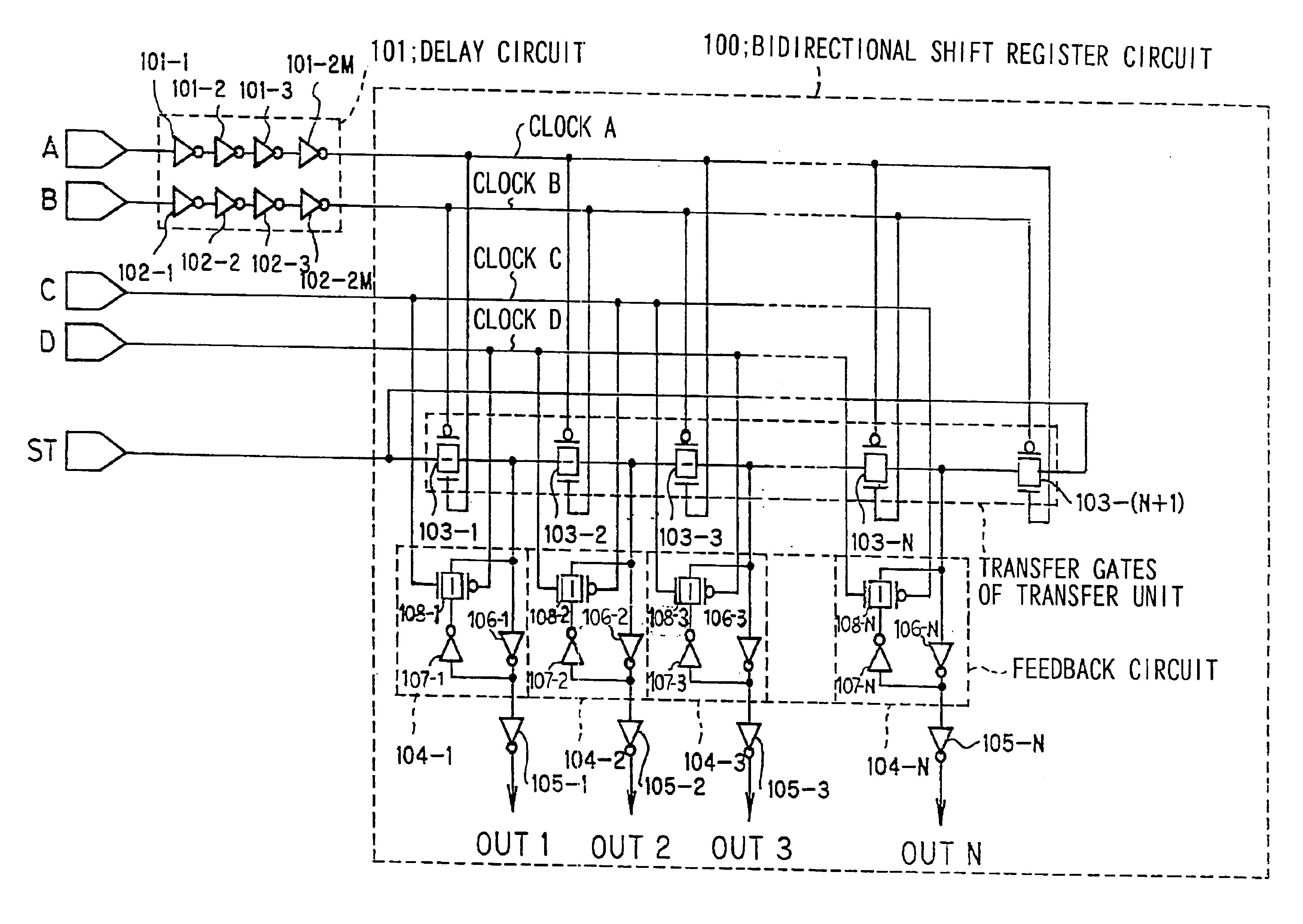
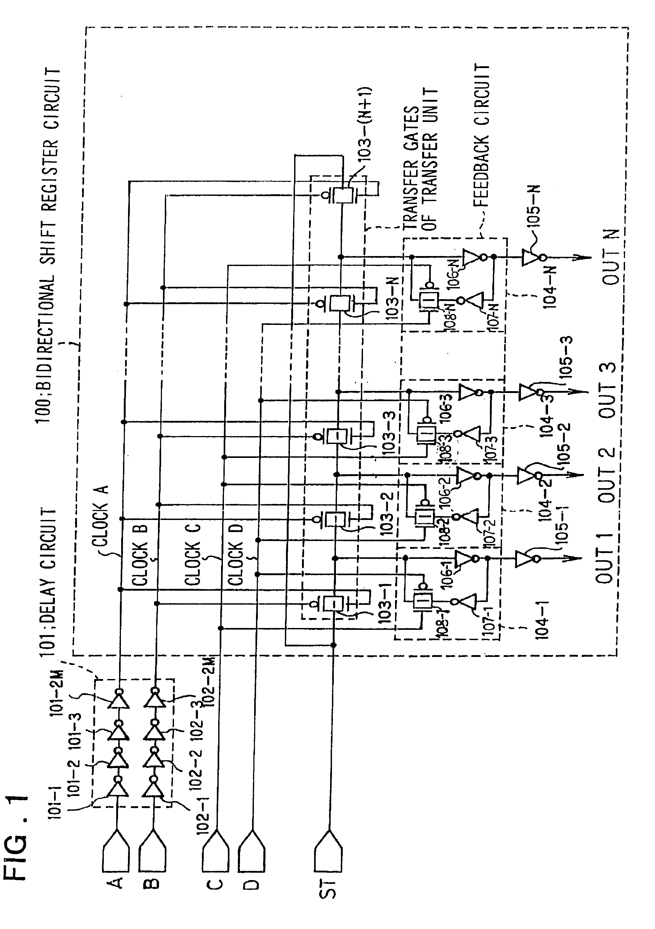
Embodiments of the present invention will now be described with reference to the drawings. FIG. 1 is a diagram showing the configuration of a first embodiment of the scanning circuit of the present invention. Referring now to FIG. 1, the scanning circuit comprises a bidirectional shift register circuit 100 which is control led by four phase clocks such as clocks A through D and a delay circuit 101 which delays the clocks A and B relative to the clocks C and D.

The bidirectional shift register circuit comprises N stages of transfer gates (CMOS transfer gate) 103-1 through 103-(N+1) of a transfer unit, which gates are in series connected for successively transferring a start pulse input to an input terminal ST to a next stage in response to clocks A and B which are stage by stage alternatingly input to the gates of n and p channel MOS transistors, feedback circuits 104-1 through 104-N which prevent the attenuation of the magnitude of the transferred pulse signals and output buffer circ...

second embodiment

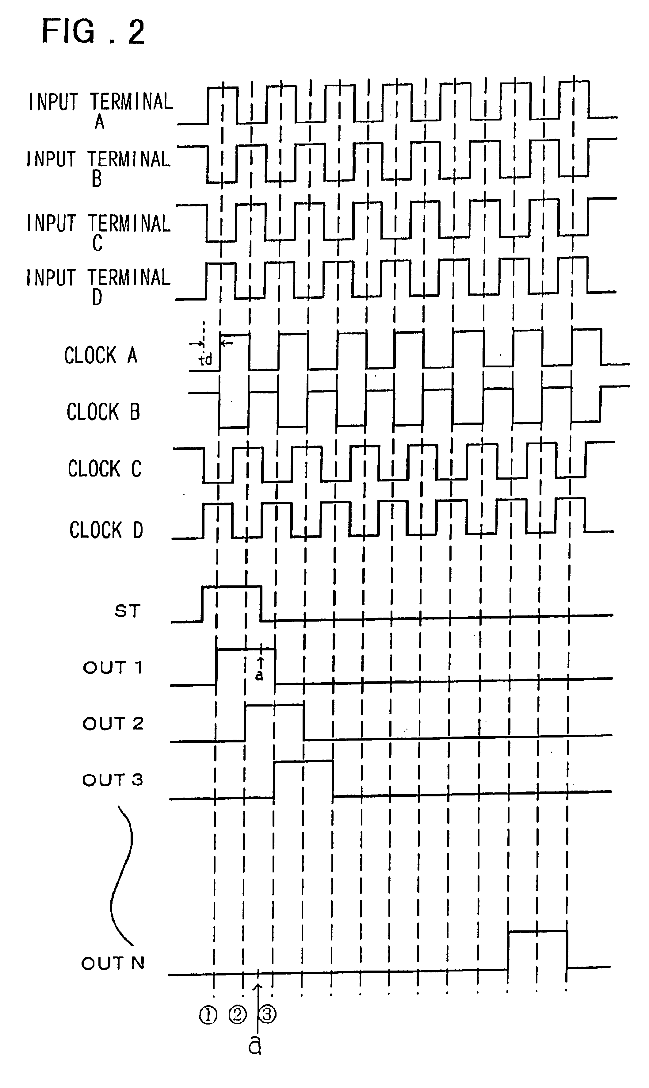
Operation of the scanning circuit of the present invention which is shown in FIG. 4 will be described with reference to timing charts of FIGS. 5 and 6.

The scanning circuit which is shown in FIG. 4 is capable of bidirectionally scanning by presetting the control clocks. Similarly to the operation of the first embodiment, transferring of the start pulse from OUT 1 to OUT N in an ascending order will be defined as rightward shift and transferring of the start pulse from OUT N to OUT 1 in an descending order will be defined as leftward shift. FIGS. 5 and 6 are timing charts explaining the timing relationships of rightward and leftward shifts of the scanning circuit in the second embodiment of the present invention, respectively.

Complementary two phase signals are input to the input terminals 1 and 2 and then distributed to the delay circuit 101 and phase inverting circuit 109. Outputs of the delay circuit 101 are used as clocks A and B for control 1 ng the transfer gates of the transfer...


PUM

PropertyMeasurementUnit
phaseaaaaaaaaaa
sizeaaaaaaaaaa
currentaaaaaaaaaa

Abstract

A scanning circuit having such a high operation margin for the phase deviation of clock signal that its operation is stable. The scanning circuit includes a bidirectional shift register having transfer gates of a transfer unit and a feedback circuit, the operation of which is control led by four phase clocks. The scanning circuit comprises a delay circuit (101) that delays control clocks (A, B) supplied to the transfer gates of the transfer unit (103) relative to control clocks (C, D) supplied to the feedback circuit (104).

Description

FIELD OF THE INVENTIONThe present invention relates to a scanning circuit and in particular to a scanning circuit which is capable of bidirectionally scanning.BACKGROUND OF THE INVENTIONFor the purpose of reducing the size and cost of liquid crystal display devices, development in technology has been made to integrate on a substrate, which is a liquid crystal display substrate, peripheral drive circuits such as data and gate driver circuits for driving data and gate lines of pixel matrices, respectively. A scanning circuit for generating gate scanning and sampling pulse signals is an essential circuit component among various circuits which constitute peripheral drive circuits.The scanning circuit should be capable of bidirectionally scanning to meet the requirements for advanced functions such as display-reversing function of the liquid crystal display. In particular, in case where the liquid crystal display is used for a liquid crystal projector system, a function of reversing an i...

Claims


Application Information

Patent Timeline
Patent Type & Authority Patents(United States)
IPC IPC(8): G02F1/133G02F1/13G09G3/36G09G3/00G09G3/20G11C19/00
CPCG09G3/3688G09G2310/0283G02F1/133
Inventor SATO, TETSUSHISEKINE, HIROYUKI
Owner VISTA PEAK VENTURES LLC
Why Eureka
Try Eureka