Design method for integrated circuit having scan function

a design method and integrated circuit technology, applied in the direction of cad circuit design, program control, instruments, etc., can solve the problems of increasing the number of man hours involved in library registration and circuit scal

Inactive Publication Date: 2006-01-24
MONTEREY RES LLC
View PDF5 Cites 18 Cited by
  • Summary
  • Abstract
  • Description
  • Claims
  • Application Information

AI Technical Summary

Benefits of technology

[0023]According to the above second aspect of the present invention, as a result of substituting the second flip flops equipped with a scan function for a plurality of standard cells and further substituting the substitute standard cell and other standard cell for a different standard cell, the surface-area increase that accompanies the addition of the second flip flops can be made smaller.

Problems solved by technology

Therefore, in order to design a logic circuit with a scan function and perform the layout thereof, a layout library (hard macro library) for the scan flip flops serving to implement the scan function is required, and there are therefore problems such as an increase in the man hours involved in the library registration.
Further, in a case where a scan circuit for implementing the scan function is introduced and this circuit is developed as a plurality of standard cells without the use of a scan flip flop layout library, there are problems such as an increase in circuit scale.

Method used


Image

  • Design method for integrated circuit having scan function
  • Design method for integrated circuit having scan function
  • Design method for integrated circuit having scan function

Examples


Embodiment Construction

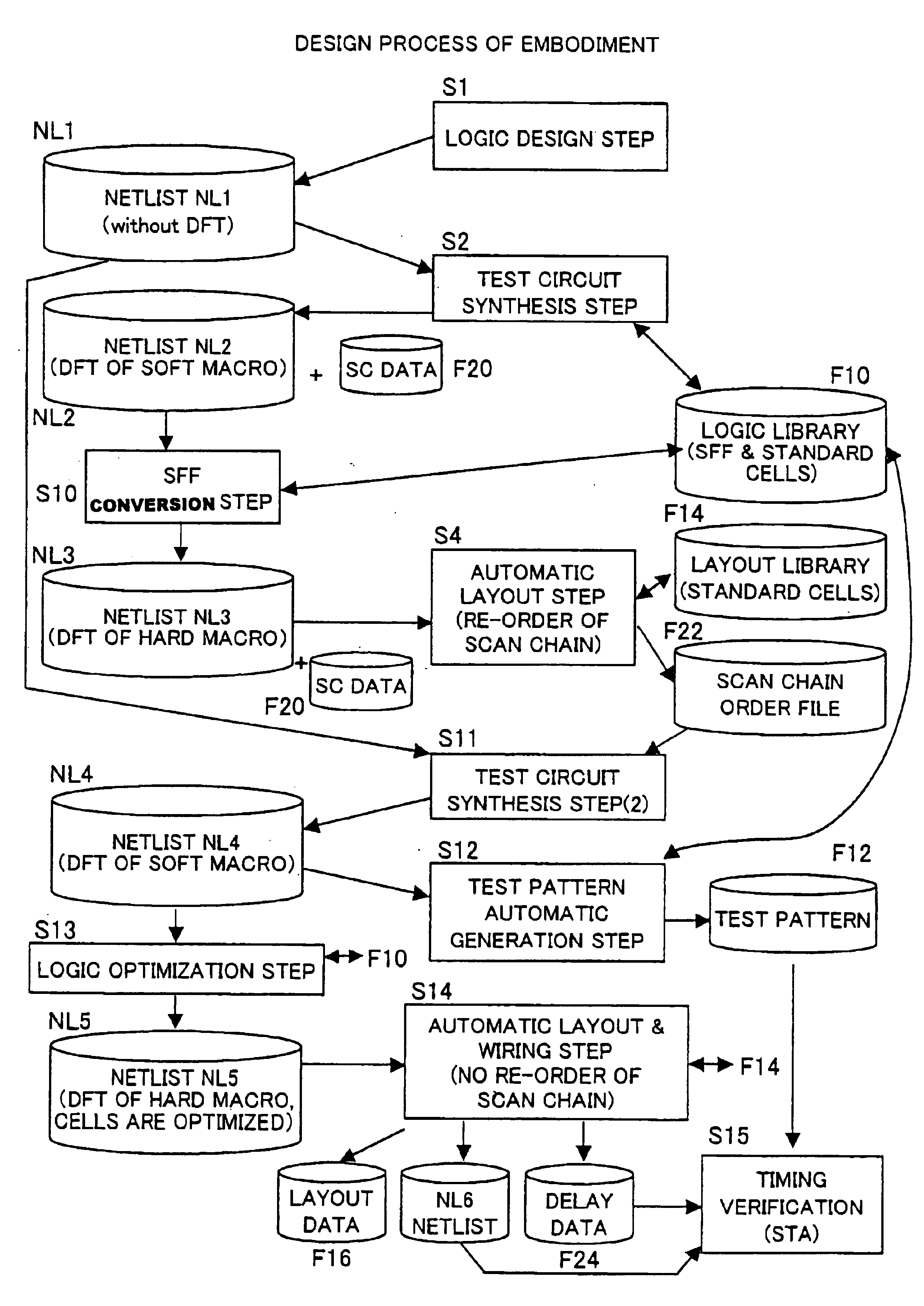
[0034]An embodiment example of the present invention will be described hereinbelow with reference to the drawings. However, the scope of protection of the present invention is not limited to or by the embodiment example below, but is instead intended to cover the inventions appearing in the claims as well as any equivalents thereof.

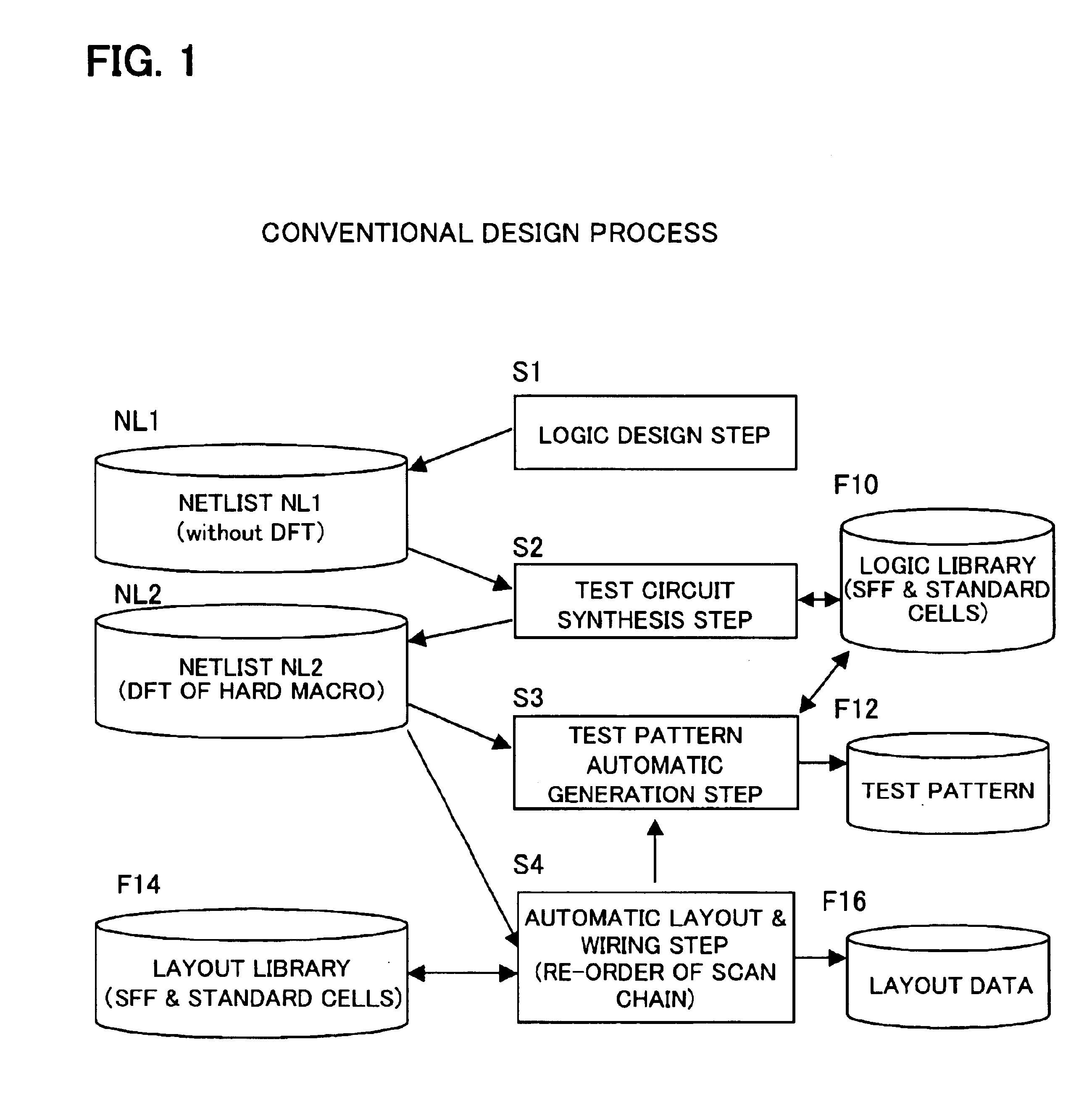
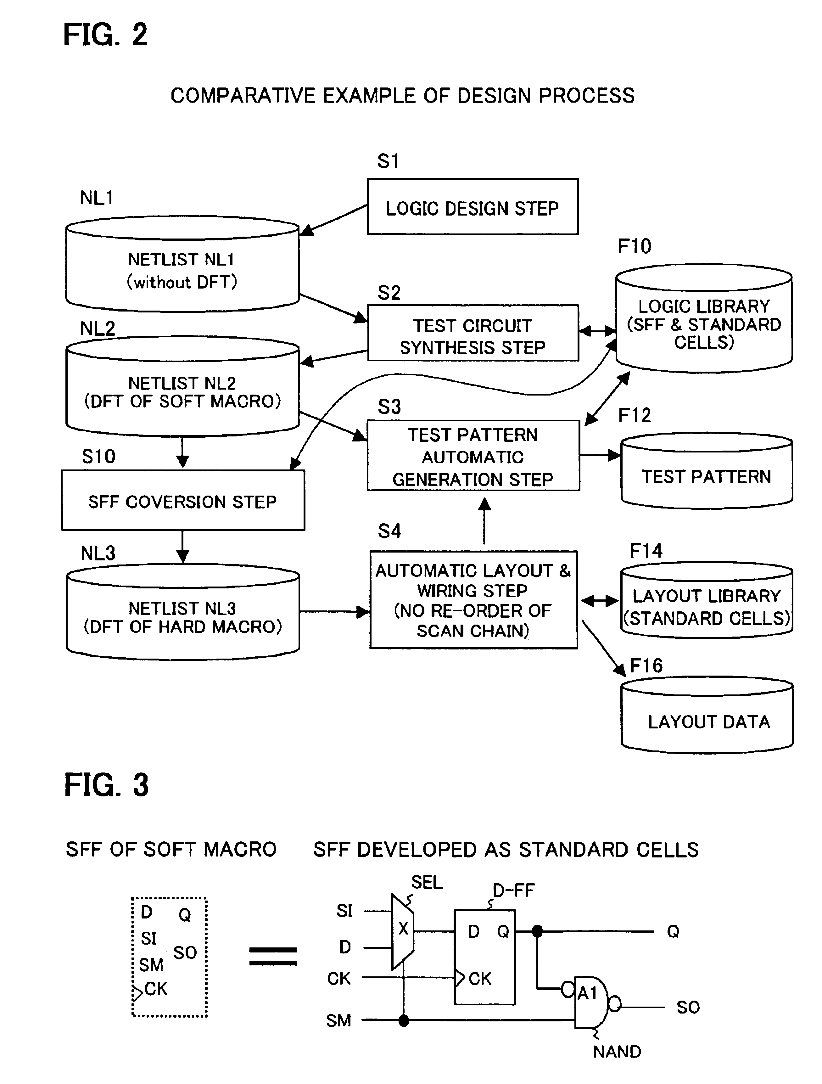
[0035]FIG. 2 is a flowchart showing design steps of a comparative example of the present embodiment. A description for the comparative example of FIG. 2 which is a partial modification of the conventional example in FIG. 1 will be provided before the present embodiment is described.

[0036]In the comparative example, the netlist NL1 generated in the logic design step S1 is converted to the netlist NL2 for a logic circuit that comprises a test circuit in which flip flops equipped with a scan function are connected by a scan chain, in the test circuit synthesis step S2. In the same way as the conventional example, in this step S2, a conversion is performed by...


PUM


Abstract

The present invention provides a method for designing LSI including a logic circuit equipped with a scan circuit without generating a hard-macro library for the scan flip flops constituting the scan circuit. According to the method, first netlist NL1 is converted into second netlist NL2 by adding scan circuit including scan flip-flops. Order data for connecting scan chain of the scan circuit is extracted from the second netlist NL2. Such second netlist NL2 is converted into third netlist NL3 including only hard-macros, and the third netlist NL3 is laid-out by re-ordering the scan chain so that the newly generated order data for is stored temporally. Fourth netlist NL4 including scan circuit formed by scan flip-flops of soft-macros is generated on the basis of the stored order data, then the fourth netlist NL4 is converted into fifth netlist NL5 by substituting the scan flip-flops of soft-macros for standard cells of hard-macros. Finally the generated fifth netlist is laid-out without re-ordering the scan chain.

Description

CROSS-REFERENCE TO RELATED APPLICATIONS[0001]This application is based upon and claims the benefit of priority from the prior Japanese Patent Application No. 2002-240729, filed on Aug. 21, 2002, the entire contents of which are incorporated herein by reference.BACKGROUND OF THE INVENTION[0002]1. Field of the Invention[0003]The present invention relates to an LSI (integrated circuit) design method, and more particularly to a design method for an integrated circuit equipped with a scan function.[0004]2. Description of the Related Art[0005]LSI design steps include a logic design step of designing a logic circuit for implementing a desired function; a step of laying out logic macros and logic cells that constitute the logic circuit, and interconnects connecting these logic cells on the basis of a netlist generated in the logic design step, and a verification step of performing timing verification for the logic circuit thus laid out, and so forth. In order to lay out the logic macros and...

Claims


Application Information

Patent Timeline
Patent Type & Authority Patents(United States)
IPC IPC(8): G06F17/50G01R31/30G01R31/3185G06F11/22H01L21/82H01L21/822H01L27/04
CPCG01R31/3016G06F17/5045G01R31/318583G01R31/31858G06F30/30
Inventor ARAKAWA, TOSHIO
Owner MONTEREY RES LLC
Why Eureka
Try Eureka