Waveguide with a three-dimensional lens

a waveguide and three-dimensional technology, applied in waveguides, waveguide type devices, instruments, etc., can solve the problems of obscuring the underlying display, and affecting the quality of the display

Inactive Publication Date: 2005-12-08
POA SANA LIQUIDATING TRUST
View PDF46 Cites 62 Cited by
  • Summary
  • Abstract
  • Description
  • Claims
  • Application Information

AI Technical Summary

Benefits of technology

[0010] In another embodiment of the apparatus, the invention includes at least a support substrate, a bottom cladding layer, a waveguide, and an optical lens. The waveguide is suitable for transmitting light and is formed upon the bottom cladding layer. The optical lens has a first end that is connected to the waveguide such that light rays can be communicated between the waveguide and the optical lens. The optical lens also has a second end that forms a front lens surface. The optical lens further has a raised region in between the first and second end, wherein the optical lens collimates the light rays such that the light rays transmitted through the front lens surface travel are parallel with the top surface of the support substrate.
[0011] In yet another embodiment of the apparatus, the invention includes at least a support substrate, a lamina of light formed over the top surface of the support substrate, a plurality of optical structures, and an optical position detection device. The plurality of optical structures form the lamina of light wherein each of the optical structures are formed of a waveguide and an optical lens. Each of the waveguides is suitable for transmitting light and are formed upon the top surface of the support substrate. Each of the optical lenses have a first end that is connected to a respective waveguide such that light rays can be communicated between the waveguide and the optical lens and a second end that forms a front lens surface. Each of the optical lenses has a raised region in between their respective first and second ends, wherein each of the optical lenses collimates the light rays such that the light rays transmitted through the front lens surface travel within a plane that is substantially coplanar to the top surface of the support substrate. The optical position detection device is optically coupled to each of the waveguides and is configured to detect data entries to the input system by determining the location of interrupts in the lamina caused when data is entered to the input system.
[0012] These and other features and advantages of the present invention will be presented in more detail in the following specification of the invention and the accompanying figures, which illustrate by way of example the principles of the invention.

Problems solved by technology

This approach has a number of problems.
Foremost, the film causes the display to appear dim and obscures viewing of the underlying display.
However, in the case of most portable devices, such as cell phones, personal digital assistants, and laptop computers, high intensity screens are usually not provided.
If they were available, the added intensity would require additional power, reducing the life of the battery of the device before recharge.
The films are also easily damaged.
In addition, the cost of the film scales dramatically with the size of the screen.
With large screens, the cost is therefore typically prohibitive.
This type of data input display, however, also has a number of problems.
The relatively large number of LEDs and photodiodes, and the need for precise alignment, make such displays complex, expensive, and difficult to manufacture.

Method used


Image

  • Waveguide with a three-dimensional lens
  • Waveguide with a three-dimensional lens
  • Waveguide with a three-dimensional lens

Examples


Embodiment Construction

[0019] The present invention will now be described in detail with reference to a few preferred embodiments thereof as illustrated in the accompanying drawings. In the following description, numerous specific details are set forth in order to provide a thorough understanding of the present invention. It will be apparent, however, to one skilled in the art, that the present invention may be practiced without some or all of these specific details. In other instances, well known operations have not been described in detail so not to unnecessarily obscure the present invention.

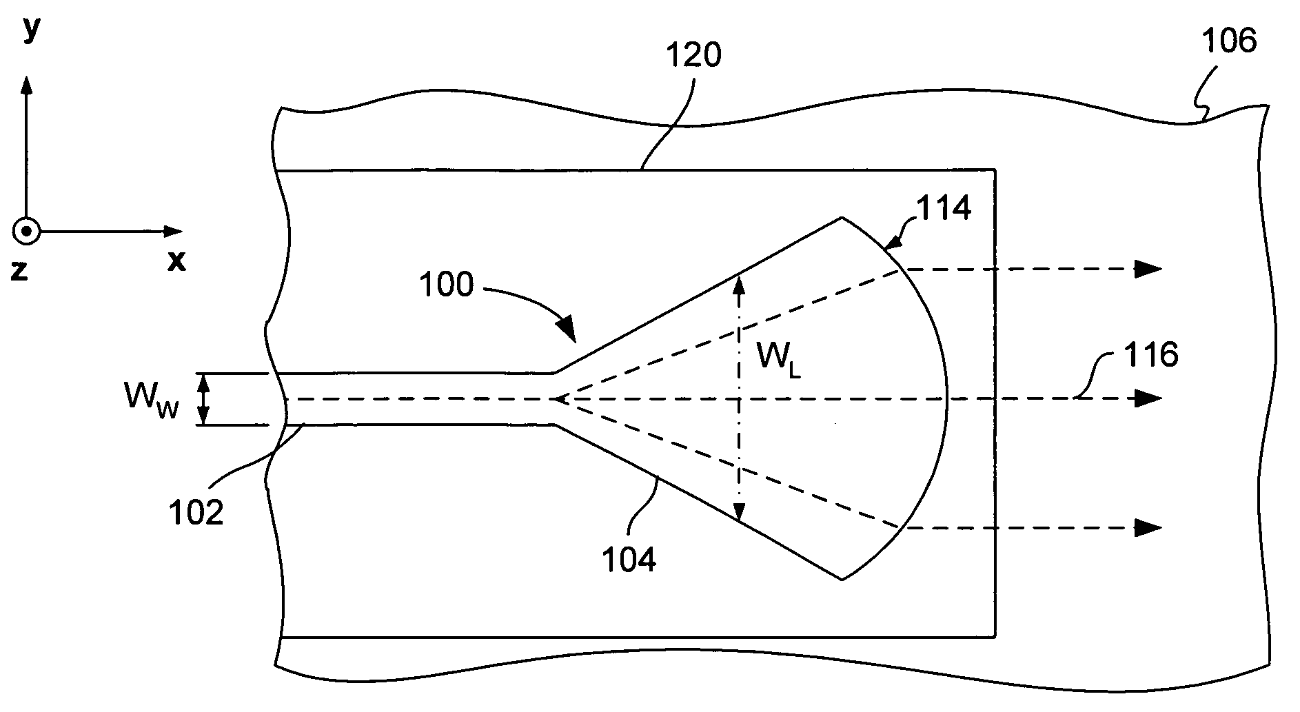
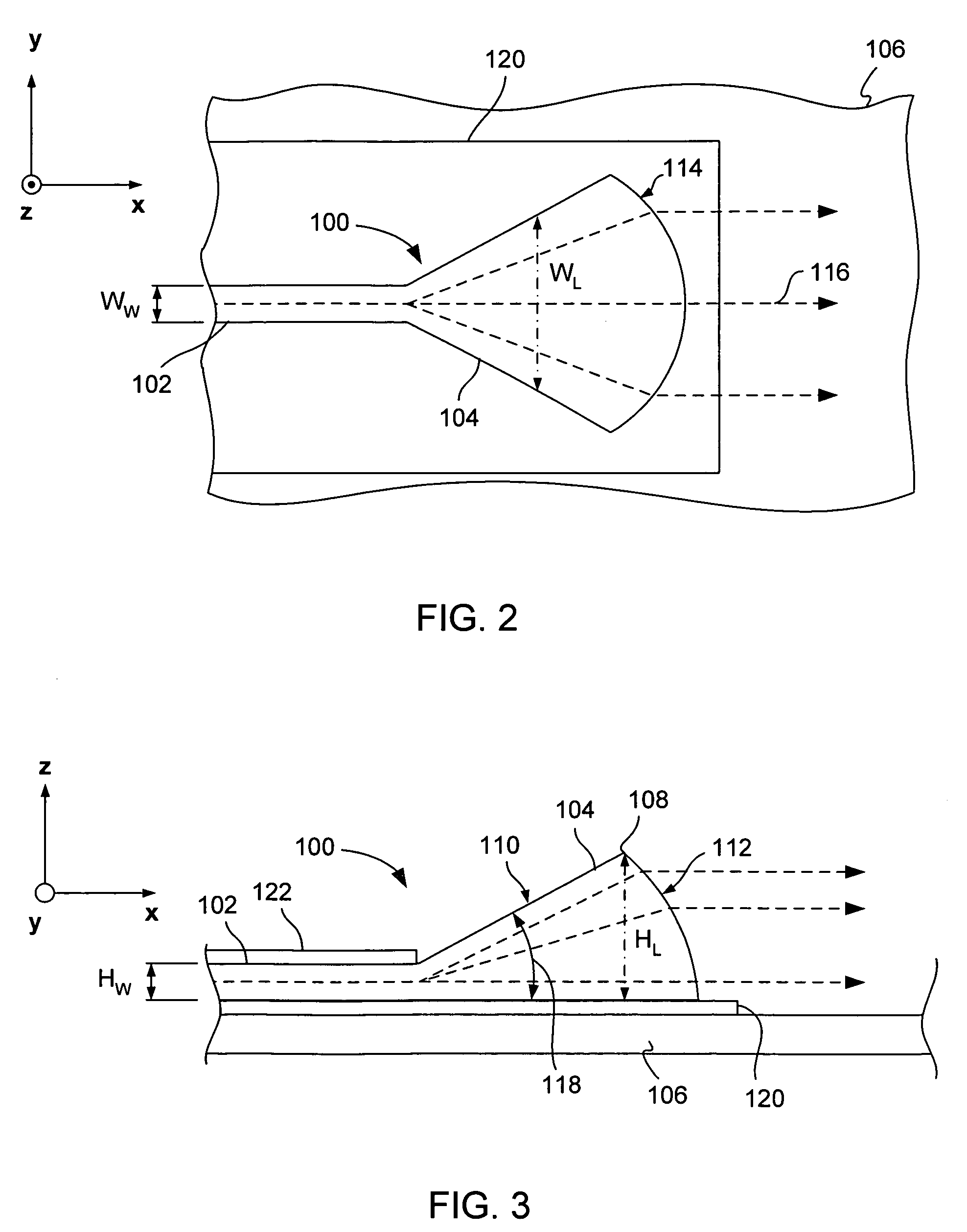
[0020] The present invention pertains to optical transmission techniques for the efficient transmission of light rays within a desired plane that is above a working surface. The techniques specifically relate to an optical transmission structure that includes a waveguide and an optical lens. The optical lens is formed on the working surface and has a sufficiently large thickness to allow the formation of a curved ...


PUM


Abstract

Optical transmission structures include a waveguide and an optical lens wherein the optical lens has a sufficiently large thickness to allow the formation of a curved front lens surface that collimates transmitted light rays so that they travel within a plane that is coplanar to a working surface. The present invention also relates to a technique for manufacturing the optical transmission structure, which involves the use of a photopolymer material. The optical transmission structure can be implemented in various systems such as a system for optical data input.

Description

CROSS-REFERENCE TO RELATED APPLICATIONS [0001] This application is related to U.S. patent application Ser. No. ______ (Attorney Docket No. NSC1P302), filed on the same date herewith and entitled “Techniques for Manufacturing a Waveguide With a Three-Dimensional Lens,” the content of which is hereby incorporated by reference. [0002] This application is also related to U.S. patent application Ser. No. ______ (Attorney Docket No. NSC1P318), filed on the same date herewith, entitled “Apparatus and Method for a Molded Waveguide for Use with Touch Screen Displays,” and to U.S. patent application Ser. No. 10 / 758,759 (Attorney Docket No. NSC1P292), filed on Jan. 15, 2004, entitled “Hybrid Waveguide,” and to U.S. patent application Ser. No. 10 / 817,564 (Attorney Docket No. GRAMP005), filed on Apr. 1, 2004, entitled “A Data Input Device Using A Light Lamina Screen and an Optical Position Digitizer,” which claims priority from U.S. Provisional Patent Application No. 60 / 461,045, filed on Apr. 8,...

Claims


Application Information

Patent Timeline
Patent Type & Authority Applications(United States)
IPC IPC(8): G02B6/42G02B6/12G02B6/122G02B6/00G02B6/32G02B6/26
CPCG02B6/12004G02B6/1221G02B6/1228G02B6/32G02B2006/12102G02B2006/1219Y10S385/901B33Y70/00G02B6/12G02B6/00G06F3/0354G02B6/138
Inventor LUO, XIAO BING
Owner POA SANA LIQUIDATING TRUST
Why Eureka
Try Eureka