

Liquid crystal display device and fabrication method thereof
a liquid crystal display and fabrication method technology, applied in optics, instruments, non-linear optics, etc., can solve the problems of reducing production yield, increasing the fabrication process of liquid crystal panels, and reducing the power consumption of lcd over that of the crt for equal screen sizes
- Summary
- Abstract
- Description
- Claims
- Application Information
AI Technical Summary
Problems solved by technology
Method used
Image

Examples
first embodiment
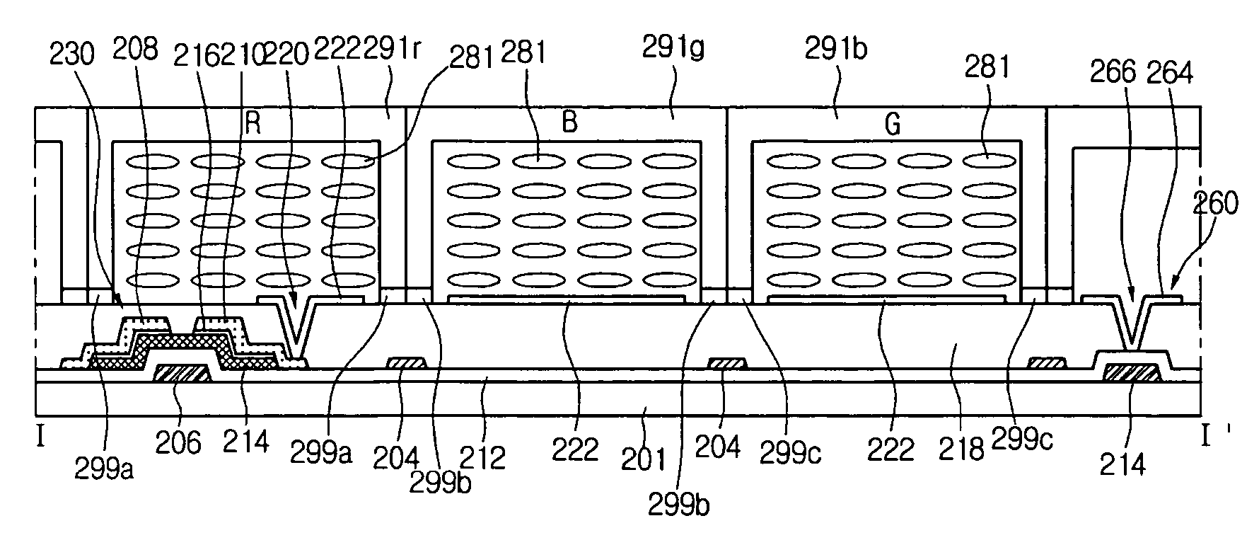
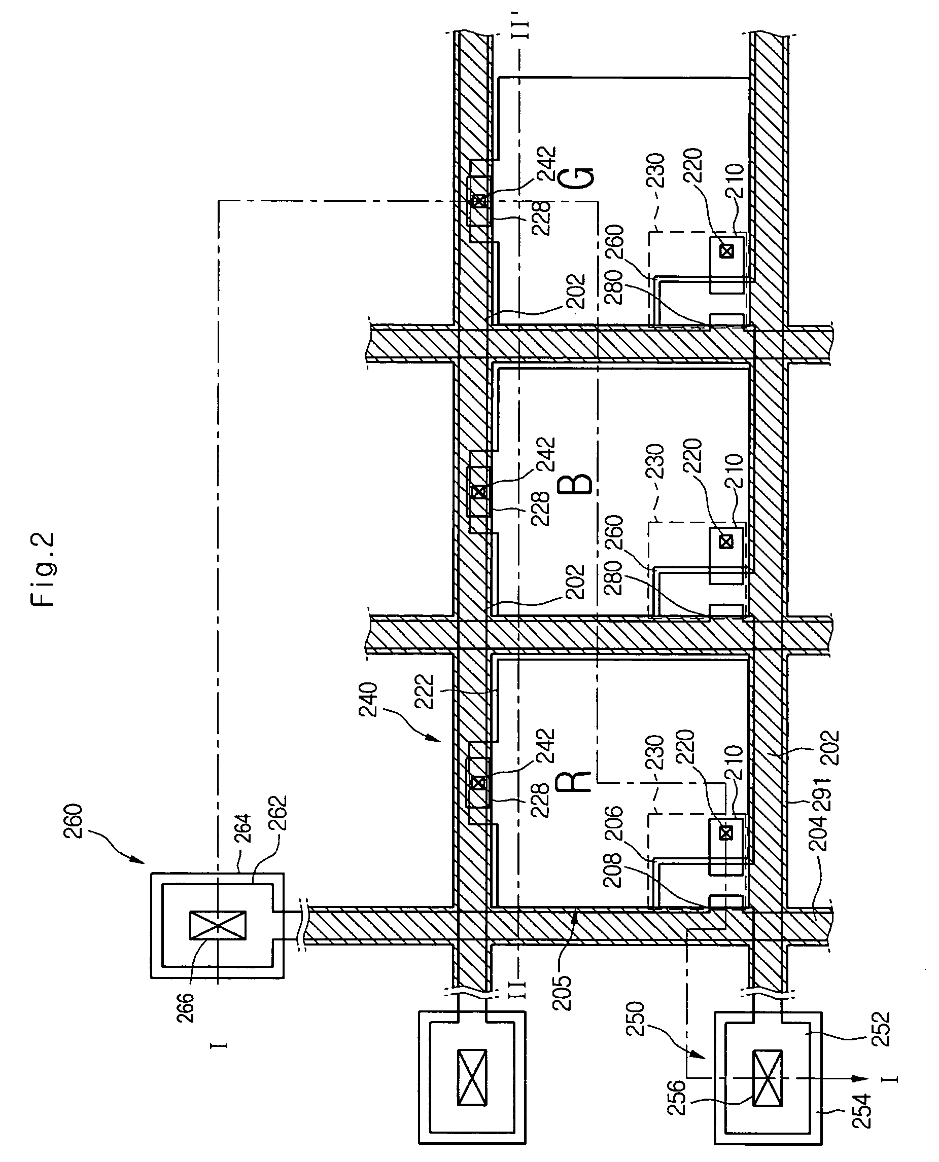
[0029]FIGS. 2 and 3 are a plan view and a sectional view of an LCD according to the present invention, respectively. Referring to FIGS. 2 and 3, upon a lower substrate 201, there are formed a gate line 202, a data line 204, a thin film transistor (TFT) 230 formed at every intersection of the gate line 202 and the data line 204, a pixel electrode 222 formed at a pixel region provided by that intersection structure, a storage capacitor 240 formed at an overlap region of the gate line 202 and a storage electrode 228, a gate pad 250 connected to the gate line 202, and a data pad 260 connected to the data line 204. Herein, the gate line 202 intersects with the data line 204, while a gate insulating layer 212 is interposed therebetween.
[0030] The gate line 202 applies a gate signal and the data line 204 applies a data signal. The gate line 202 and the data line 204 are formed in a shape of an intersection structure, to thereby define a pixel region 205.
[0031] The TFT 230 maintains the ch...
second embodiment
[0059]FIGS. 5A to 5E are sectional views illustrating a method for fabricating an LCD according to the present invention. Herein, like reference numerals in the drawings denote like elements so that detail descriptions for those elements, which are identical to the elements illustrated in FIGS. 4A to 4H, are omitted.
[0060] To begin with, referring to FIG. 5A, a seed 399 is formed at boundaries of a red, a green and a blue pixel regions on a lower substrate 301. The seed 399 comprises a polymer material and is formed at the boundaries of the pixel regions of the lower substrate 301 by a method using a stamp 398 or a mold. The method for forming the seed 399 on the lower substrate 301 may employ a printing method using a silk screen, a transcription method of a pattern, or an imprinting method.
[0061] The seed 399 may be formed of a polymer material containing a black resin. The seed 399 may be formed in a black matrix pattern, i.e., region of a gate line, data line, a boundary of a p...
third embodiment
[0077] Detail descriptions regarding a method for fabricating the liquid crystal panel having the above structure will be set forth hereinafter as illustrated in FIGS. 7A to 7E. FIGS. 7A to 7E are sectional views illustrating a method for fabricating the LCD according to the present invention. Herein, an explanation for the fabrication of the TFT is omitted but detail illustrations focus on processes of forming a liquid crystal film and a reactive liquid crystal substrate.
[0078] Though it is not shown in the drawings, gate and data interconnections are formed on an array substrate, while the gate and data lines intersect each other. In addition, the LCD contains a TFT provided with a gate electrode extended from the gate interconnection, a gate insulating layer formed over entire the structure having the gate electrode, a semiconductor layer formed on the gate insulating layer, and source / drain electrodes formed on the semiconductor layer. A pixel electrode is connected to the drain...
PUM
| Property | Measurement | Unit |
|---|---|---|
| Color | aaaaa | aaaaa |
| Structure | aaaaa | aaaaa |
| Phase | aaaaa | aaaaa |
Abstract
Description
Claims
Application Information