Thin film device transfer method, thin film device, thin film integrated circuit device, active matrix board, liquid crystal display, and electronic apparatus

a technology of integrated circuits and thin films, applied in the direction of manufacturing tools, instruments, welding/soldering/cutting articles, etc., can solve the problems of glass substrate, increased product cost, relatively heavy and fragile,

Inactive Publication Date: 2005-04-12
SAMSUNG ELECTRONICS CO LTD
View PDF15 Cites 269 Cited by
  • Summary
  • Abstract
  • Description
  • Claims
  • Application Information

AI Technical Summary

Benefits of technology

In view of the foregoing, it is a general object of the present invention to provide a novel technique in which a substrate employed for thin film device formation and a substrate used as an actual element of a product (i.e., a substrate having characteristics desirable for usage of the product) can be selected individually and flexibly and in which thin film devices can be transferred to the substrate used as the actual product element while maintaining the layering relationship of the thin film devices with respect to the substrate employed for thin film device formation.
Through use of the technique mentioned above, a liquid crystal display device can be manufactured. For example, it is possible to realize a liquid crystal display comprising a plastic substrate, which can be curved flexibly.

Problems solved by technology

However, the quartz glass or heat-resistant glass substrate is very expensive, resulting in an increase in product cost.
The glass substrate is also disadvantageous in that it is relatively heavy and fragile.
In actuality, however, the glass substrate is heavy, not resistant to deformation, and vulnerable to dropping.
In other words, there is a discrepancy between restrictive conditions required for a manufacturing process and characteristics desirable for a manufactured product.
It has been extremely difficult to satisfy both of these required process conditions and desirable product characteristics.
On the contrary, where the object-of-transfer layer containing thin film device and electrodes is transferred to the destination-of-transfer part, the electrodes are covered with the destination-of-transfer part, making it difficult to arrange wiring connections or contacts thereon.

Method used


Image

  • Thin film device transfer method, thin film device, thin film integrated circuit device, active matrix board, liquid crystal display, and electronic apparatus
  • Thin film device transfer method, thin film device, thin film integrated circuit device, active matrix board, liquid crystal display, and electronic apparatus
  • Thin film device transfer method, thin film device, thin film integrated circuit device, active matrix board, liquid crystal display, and electronic apparatus

Examples


first embodiment

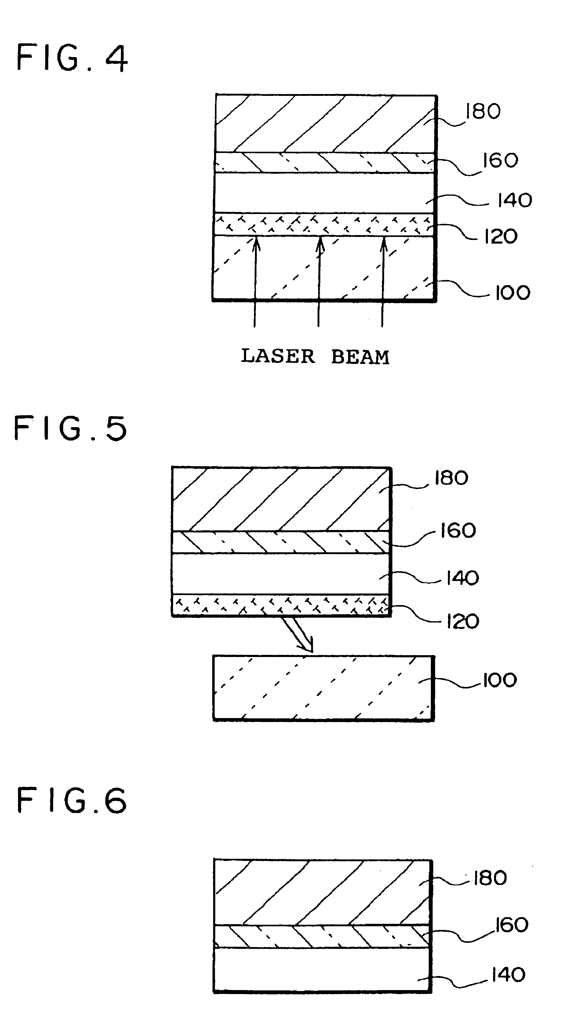
FIGS. 1 to 9 are diagrammatic illustrations for explaining a first embodiment (thin film device transfer method) according to the present invention.

[Step 1]

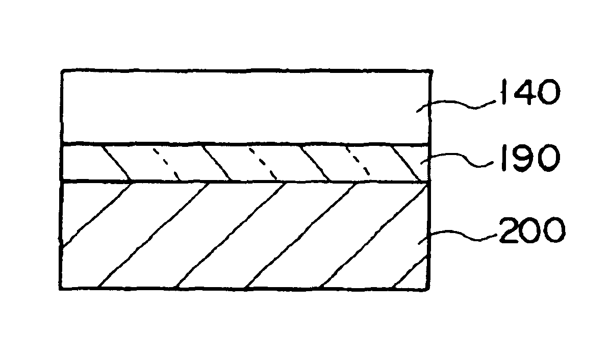
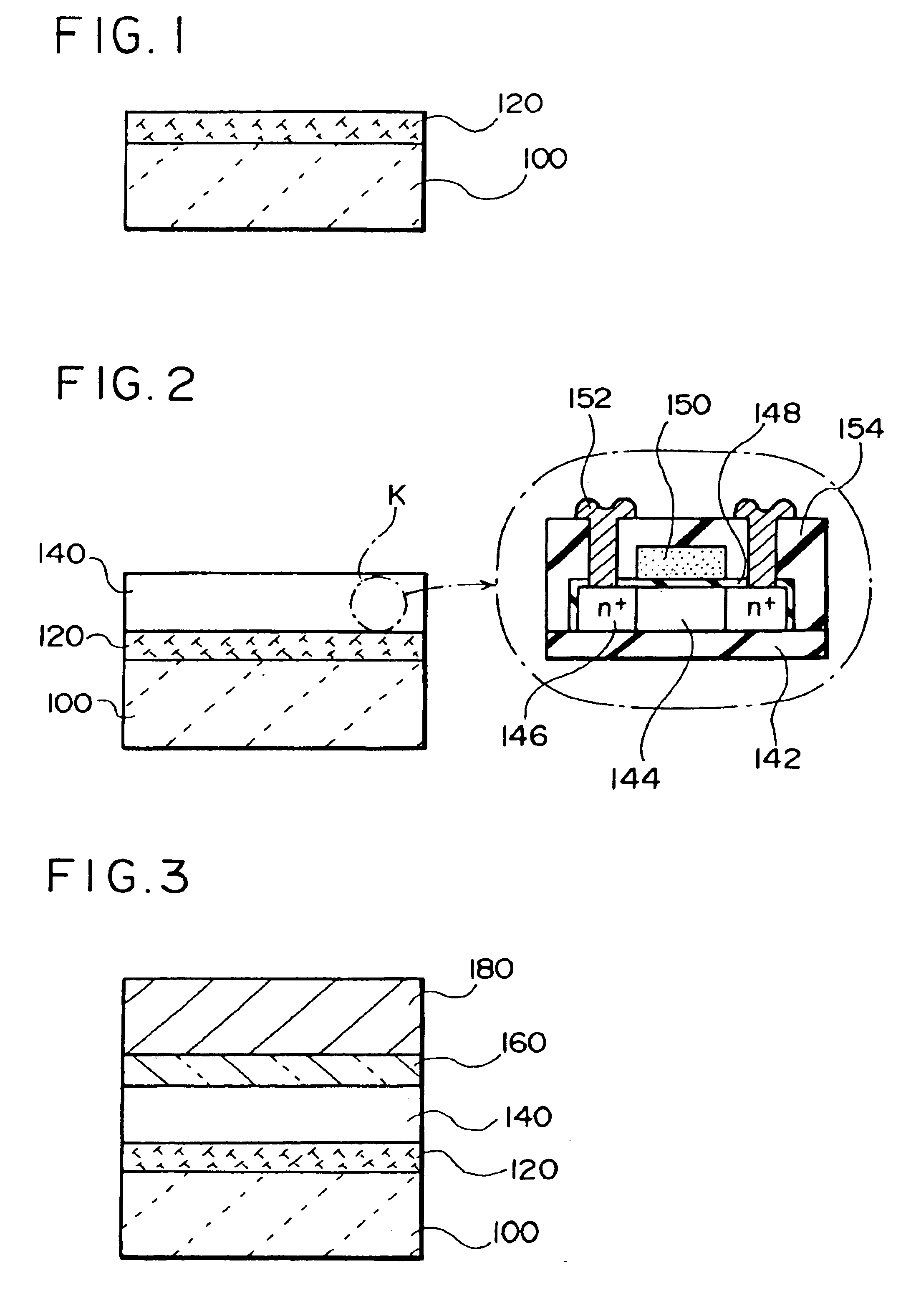
An shown in FIG. 1, a first separation layer (light absorbing layer) 120 is formed on a substrate 100. The following describes the substrate 100 and the first separation layer 120.

(1) Description of Substrate 100

The substrate 100 preferably has a property that allows transmission of light therethrough. Transmittance of light passing though the substrate 100 is preferably 10% or higher, and more preferably 50% or higher. If the transmittance is too low, attenuation (loss) of light increases to make it necessary to apply a larger amount of light for exfoliating the first separation layer.

Further, the substrate 100 is preferably made of a highly reliable material. More particularly, it is preferable that the substrate 100 be made of a heat-resisting material. The reason for this requirement is as follows: For instance, in the format...

second embodiment

With reference to FIGS. 11 to 21, the following describes a specific example of a fabrication process in which CMOS-structure TFT devices are formed on a substrate and transferred to a destination-of-transfer part.

[Step 1]

As shown in FIG. 11, a first separation layer (e.g., an amorphous silicon layer formed using the LPCVD method) 120, an intermediate layer (e.g., SiO2 film) 142, and an amorphous silicon layer (e.g., a layer formed using the LPCVD method) 143 are formed successively on a substrate (e.g., quartz substrate) 100. Then, the entire surface of the amorphous silicon layer 143 is irradiated with a laser beam for annealing. The amorphous silicon layer 143 is thus recrystallized to become a polysilicon layer.

[Step 2]

Then, as shown in FIG. 12, the laser-annealed polysilicon layer is patterned to provider islands 144a and 144b.

[Step 3]

As shown in FIG. 13, gate insulation films 148a and 148b are formed to cover the islands 144a and 144b using a CVD method, for example.

[Step 4]

A...

third embodiment

Using the technique described in the abovementioned first and second embodiments, it is possible to form a microcomputer comprising thin film devices on a desired circuit board as shown in FIG. 25A.

In FIG. 25A, a CPU 300 of which circuit is structured using thin film devices, a RAM 320, an input / output circuit 360 and a solar battery 340 having amorphous silicon PIN junctions for supplying a power voltage thereto are mounted on a flexible circuit board 182 used as a secondary destination-of-transfer part made of a material such as plastic.

Since the microcomputer shown in FIG. 25A is formed on the flexible board 182 used as the secondary destination-of-transfer part, it may be curved as shown in FIG. 25B. Flexible and light in weight, the microcomputer is invulnerable to dropping. Further, the plastic board 182 may be provided for common use as a casing part of an electronic apparatus. It is thus possible to manufacture an electronic apparatus comprising thin film devices transferred...


PUM

PropertyMeasurementUnit
wavelengthaaaaaaaaaa

Abstract

A thin film device fabrication method in which a thin film device formed on a substrate are transferred to a primary destination-of-transfer part and then the thin film device is transferred to a secondary destination-of-transfer part. A first separation layer (120) made of such a material as amorphous silicon is provided on a substrate (100) which allows passage of laser. A thin film device (140) such as TFTs are formed on the substrate (100). Further, a second separation layer (160) such as a hot-melt adhesive layer is formed on the thin film devices (140), and a primary destination-of-transfer part (180) is mounted thereon. The bonding strength of the first separation layer is weakened by irradiation with light, and the substrate (100) is removed. Thus, the thin film device (140) is transferred to the primary destination-of-transfer part. Then, a secondary destination-of-transfer part (200) is attached onto the bottom of an exposed part of the thin film device (140) via an adhesive layer (190). Thereafter, the bonding strength of the second separation layer is weakened by such means as thermal fusion, and the primary destination-of-transfer part is removed. In this manner, the thin film device (140) can be transferred to the secondary destination-of-transfer part (200) while maintaining layering relationship with respect to the substrate (100).

Description

TECHNICAL FIELDThe present invention relates to a thin film device transfer method, a thin film device, a thin film integrated circuit device, an active matrix board, a liquid crystal display, and an electronic apparatus.BACKGROUND ARTIn the manufacture of a liquid crystal display comprising thin film transistors (TFTs), for instance, thin film transistors are formed on a substrate through CVD or any other process. Since a fabrication process for forming thin film transistors on a substrate involves high-temperature treatment, a substrate made of a heat-resistant material is required, i.e., the substrate material must have a high softening point and a high melting point. At present, therefore, quartz glass is used as a material to provide a substrate capable of withstanding up to approx. 1000° C., or heat-resistant glass is used as a material to provide a substrate capable of withstanding up to approx. 500° C.As mentioned above, the substrate on which thin film devices are to be mou...

Claims


Application Information

Patent Timeline
Patent Type & Authority Patents(United States)
IPC IPC(8): H01L21/762H01L21/20H01L21/70H01L29/66H01L21/02H01L29/786H01L21/84G02F1/13G02F1/1362G02F1/136G02F1/1368H01L21/336H01L21/77H01L27/12
CPCB23K26/409H01L21/2007H01L21/76264B23K26/0063H01L27/1214H01L27/1266H01L29/78603G02F1/13454G02F1/1362H01L21/76275H01L21/76289H01L2221/68359H01L2221/68368H01L21/76283B23K26/40B23K26/57B23K2103/172H01L27/12
Inventor INOUE, SATOSHISHIMODA, TATSUYAMIYAZAWA, WAKAO
Owner SAMSUNG ELECTRONICS CO LTD
Why Eureka
Try Eureka