Liquid crystal display device

a liquid crystal display device and display defect technology, applied in static indicating devices, instruments, optics, etc., can solve problems such as the deterioration of the characteristics of transistors formed of non-crystalline semiconductors, and achieve the suppression of the display defect of liquid crystal display devices caused by a shift register malfunction

Inactive Publication Date: 2008-03-13
SEMICON ENERGY LAB CO LTD
View PDF27 Cites 266 Cited by
  • Summary
  • Abstract
  • Description
  • Claims
  • Application Information

AI Technical Summary

Benefits of technology

[0080] By using the present invention, deterioration in characteristics of a transistor can be suppressed. Therefore, a malfunction of a shift register caused by deterioration in characteristics of the transistor can be prevented. In addition, a display defect of a liquid crystal display device caused by a malfunction of the shift register can be suppressed.

Problems solved by technology

However, it is known that characteristics of a transistor formed of a non-crystalline semiconductor deteriorate in accordance with the amount of time for which the transistor is turned on, voltage applied, or the like.
Among causes of deterioration, a threshold voltage shift where the threshold voltage is shifted (raised) is one of the major causes of a malfunction of a shift register.

Method used


Image

  • Liquid crystal display device
  • Liquid crystal display device
  • Liquid crystal display device

Examples


embodiment mode 1

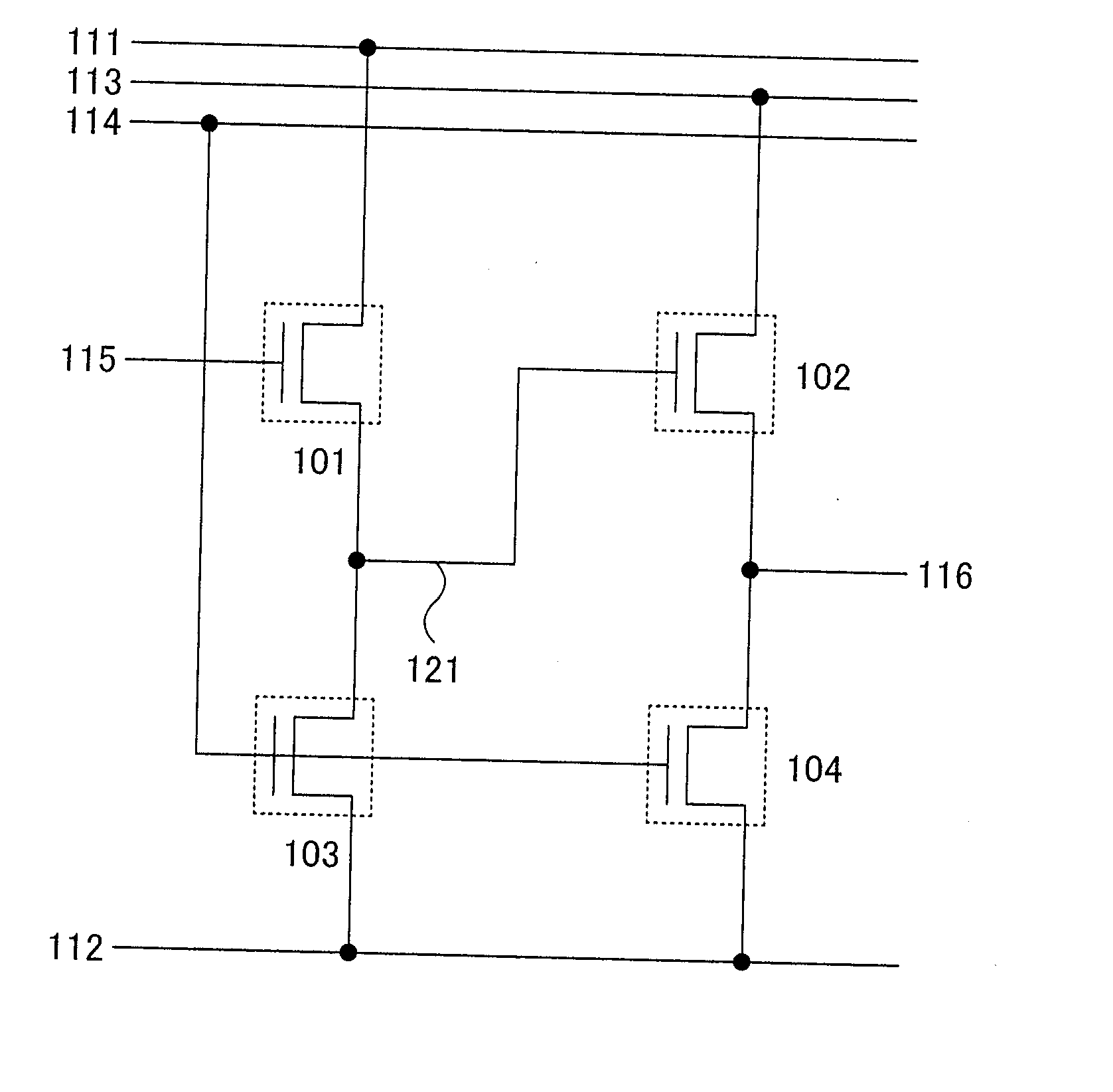
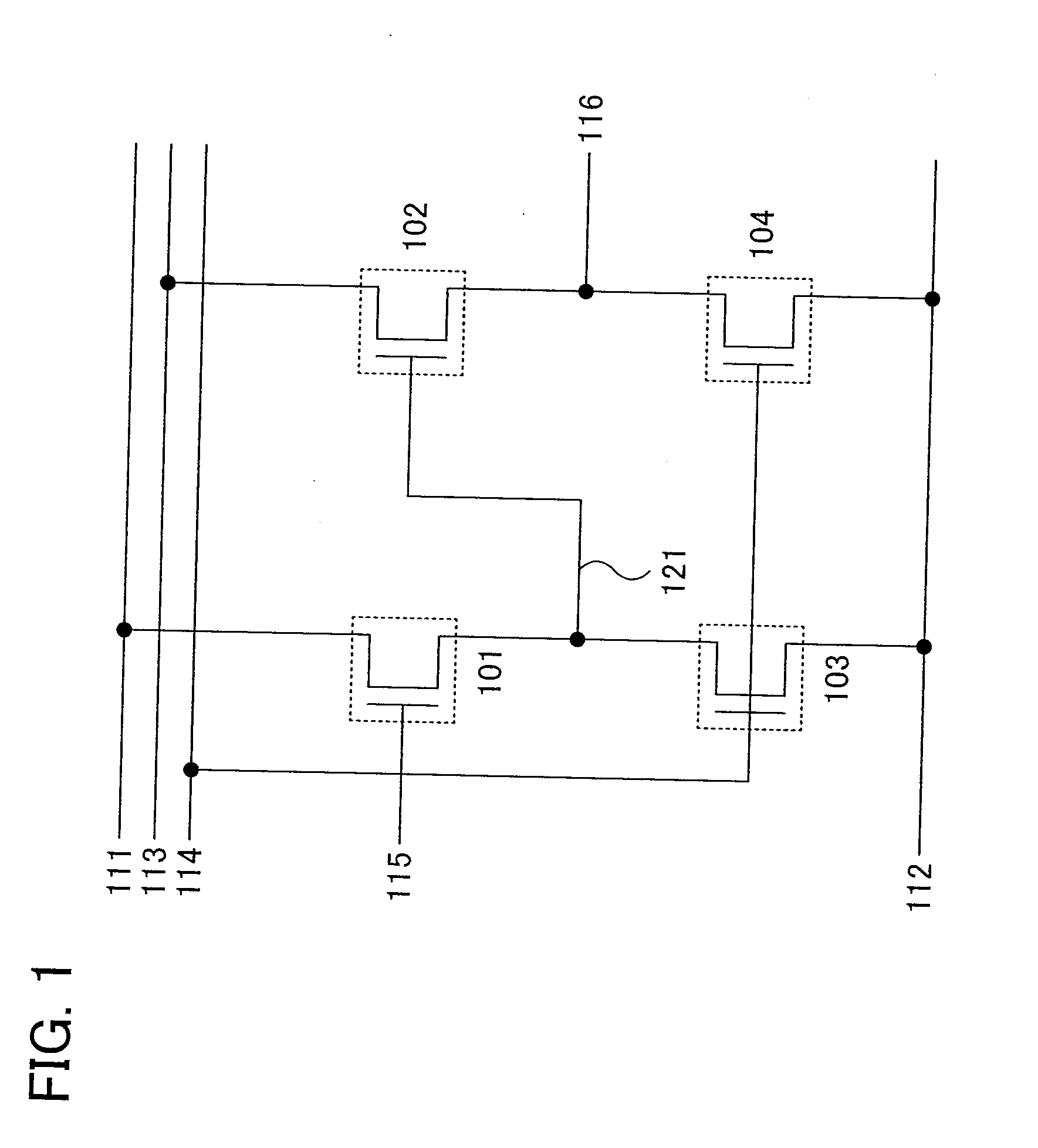
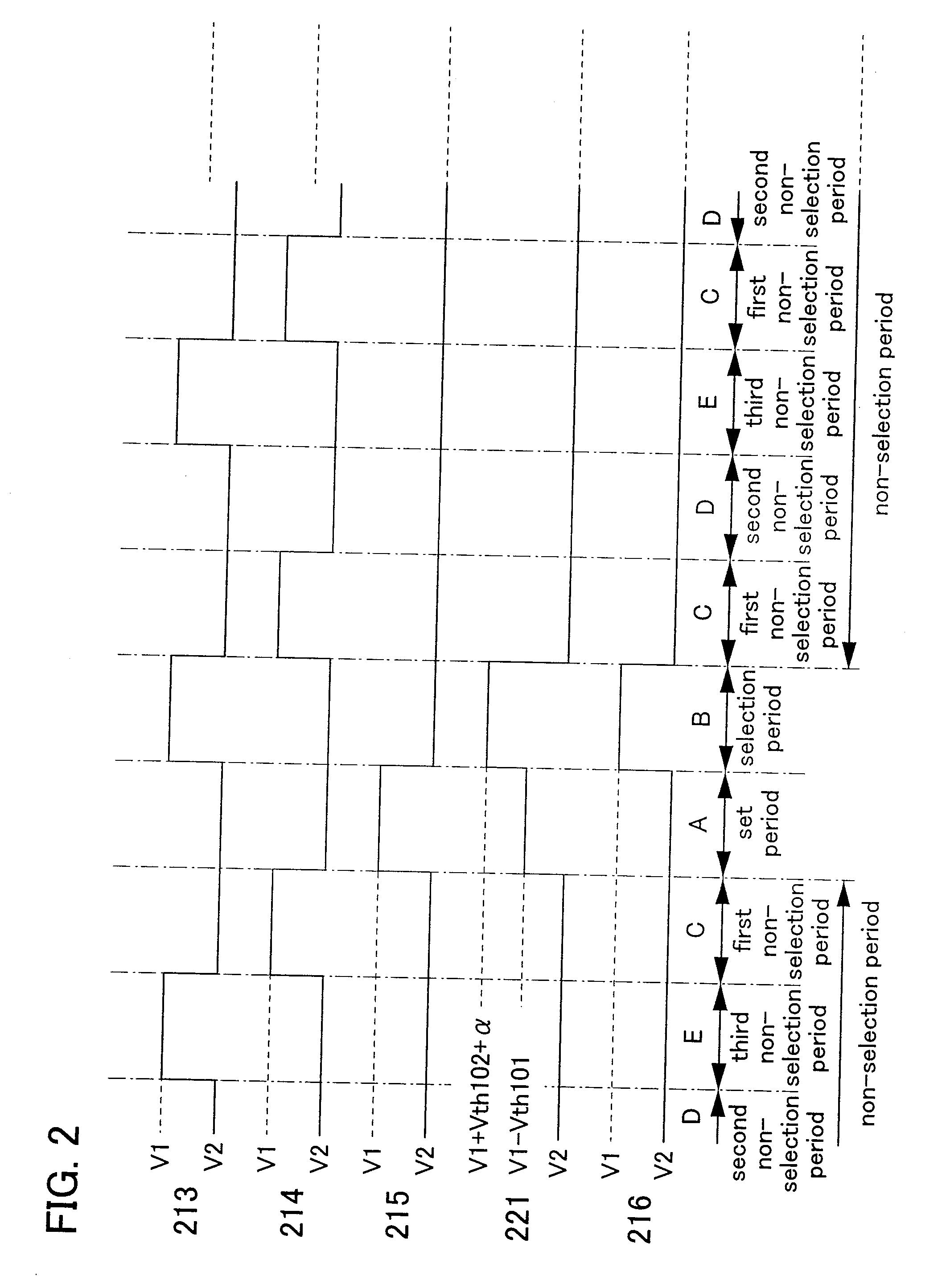
[0188] In this embodiment mode, a basic structure of a shift register of a display device of the present invention is described with reference to drawings. FIG. 1 shows a flip-flop of one stage (e.g., a first stage), which is one of a plurality of flip-flops included in a shift register. The flip-flop shown in FIG. 1 includes a first transistor 101, a second transistor 102, a third transistor 103, and a fourth transistor 104. Note that the flip-flop is connected to a first wiring 111, a second wiring 112, a third wiring 113, a fourth wiring 114, a fifth wiring 115, and a sixth wiring 116. In this embodiment mode, each of the first transistor 101, the second transistor 102, the third transistor 103, and the fourth transistor 104 is an N-channel transistor and is turned on when gate-source voltage (Vgs) exceeds the threshold voltage (Vth). Note that the first wiring 111 and the second wiring 112 may be called a first power supply line and a second power supply line, respectively. In a...

embodiment mode 2

[0256] In this embodiment mode, a flip-flop having a structure which is different from that of Embodiment Mode 1 is shown in FIG. 13. Note that portions which are similar to Embodiment Mode 1 are denoted by common reference numerals and detailed description of the portions which are the same and portions which have similar functions is omitted.

[0257] The flip-flop shown in FIG. 13 includes the first transistor 101, the second transistor 102, the third transistor 103, the fourth transistor 104, and a fifth transistor 1305. Note that the flip-flop is connected to the first wiring 111, the second wiring 112, the third wiring 113, the fourth wiring 114, the fifth wiring 115, the sixth wiring 116, and a seventh wiring 1317. In this embodiment mode, the fifth transistor 1305 is an N-channel transistor and is turned on when gate-source voltage (Vgs) exceeds the threshold voltage (Vth). Note that the seventh wiring 1317 may be called a third signal line.

[0258] The first terminal (one of t...

embodiment mode 3

[0281] In this embodiment mode, a flip-flop having a structure which is different from those of Embodiment Modes 1 and 2 is shown in FIG. 19. Note that portions which are similar to Embodiment Modes 1 and 2 are denoted by common reference numerals and detailed description of the portions which are the same and portions which have similar functions is omitted.

[0282] The flip-flop shown in FIG. 19 includes the first transistor 101, the second transistor 102, the third transistor 103, the fourth transistor 104, the fifth transistor 1305, a sixth transistor 1906, a seventh transistor 1907, an eighth transistor 1908, and a ninth transistor 1909. Note that the flip-flop is connected to the first wiring 111, the second wiring 112, the third wiring 113, the fourth wiring 114, the fifth wiring 115, the sixth wiring 116, and the seventh wiring 1317. In this embodiment mode, each of the sixth transistor 1906, the seventh transistor 1907, the eighth transistor 1908, and the ninth transistor 19...


PUM


Abstract

A first transistor, a second transistor, a third transistor, a fourth transistor are provided. In the first transistor, a first terminal is electrically connected to a first wiring; a second terminal is electrically connected to a gate terminal of the second transistor; a gate terminal is electrically connected to a fifth wiring. In the second transistor, a first terminal is electrically connected to a third wiring; a second terminal is electrically connected to a sixth wiring. In the third transistor, a first terminal is electrically connected to a second wiring; a second terminal is electrically connected to the gate terminal of the second transistor; a gate terminal is electrically connected to a fourth wiring. In the fourth transistor, a first terminal is electrically connected to the second wiring; a second terminal is electrically connected to the sixth wiring; a gate terminal is connected to the fourth wiring.

Description

BACKGROUND OF THE INVENTION [0001] 1. Field of the Invention [0002] The present invention relates to a liquid crystal display device. In particular, the present invention relates to a liquid crystal display device having a shift register formed by using a transistor. In addition, the present invention relates to a method for driving the liquid crystal display device. Further, the present invention relates to an electronic device having the liquid crystal display device in a display portion. [0003] 2. Description of the Related Art [0004] In recent years, with the increase of large display devices such as liquid crystal televisions, liquid crystal display devices have been actively developed. In particular, a technique for forming a pixel circuit and a driver circuit including a shift register or the like (hereinafter also referred to as an internal circuit) over the same insulating substrate by using transistors formed of a non-crystalline semiconductor (hereinafter also referred to...

Claims


Application Information

Patent Timeline
Patent Type & Authority Applications(United States)
IPC IPC(8): G09G3/36
CPCG02F1/133753H01L27/1255G02F2001/133622G09G3/342G09G3/3655G09G3/3674G09G3/3685G09G2310/024G09G2320/0252G11C19/28H01L27/06H01L27/15H01L27/1225H01L27/124G02F1/1393G02F1/133622H10K59/351H10K59/352A42B1/02A42B1/004A42B1/008A42B1/24A42C5/02H10K50/8426H10K59/35H10K59/123H10K59/124H10K59/131H10K59/1213H10K59/1216H10K71/00H10K2102/3023H10K2102/3026H10K2102/3031G02F1/136213G02F1/136286H01L29/247H01L29/78693G02F1/13306G02F1/13452G02F1/1368G02F2202/103G09G3/3677G09G2300/0426G09G2300/0452G09G2310/0286G09G2310/08G09G2330/021H01L21/67167H01L27/1222H01L27/156
Inventor UMEZAKI, ATSUSHI
Owner SEMICON ENERGY LAB CO LTD
Why Eureka
Try Eureka