Handling of write transactions in a data processing apparatus

a data processing apparatus and write transaction technology, applied in the direction of data processing input/output process, electric digital data processing, instruments, etc., to achieve the effect of reducing the complexity of the apparatus

Active Publication Date: 2005-12-08
ARM LTD
View PDF1 Cites 14 Cited by
  • Summary
  • Abstract
  • Description
  • Claims
  • Application Information

AI Technical Summary

Benefits of technology

[0010] In accordance with the present invention, the bus master interface is allowed to generate a write transaction such that the write data is received at the bus slave interface before the associated write address. This is counterintuitive, as the slave device responsible for storing the write data at the write address clearly cannot store the write data until the write address is received. Nevertheless, by allowing the write data to be received before the associated write address, the complexity of the apparatus can be significantly reduced, since there is no longer the requirement to include additional logic at each interface to re-align write data with the write address.
[0013] It will be appreciated that the bus circuitry can take a variety of forms. However, in one embodiment, the bus circuitry comprises an interconnect circuit providing an address channel for transfer of said write address and a separate write data channel for transfer of said write data. The address channel can utilise different physical connection paths to those used by the write data channel. Hence, such an interconnect circuit is one example of bus circuitry where the write address may take longer to be propagated from the bus master interface to the bus slave interface than may the associated write data, due to the different physical connection paths provided for the address channel and the write data channel, and hence where utilisation of the present invention avoids the need for additional logic to re-align the write data to the write address.
[0014] In one particular embodiment, each address channel and each write data channel is provided over one of said connection paths, at least one of the connection paths including one or more storage elements therein for temporarily storing data transferred by that connection path, the number of storage elements in the connection path of the address channel exceeding the number of storage elements in the connection path of the write data channel, thereby causing the write data to be received at the bus slave interface before the associated write address. Such storage elements are used to section a particular connection path into a number of path portions, with the signals propagated along that connection path then passing over one path portion during each clock cycle. The use of such storage elements can hence assist in enabling the interconnect circuit to meet the timing requirements of the apparatus in which that interconnect circuit is used, by ensuring that each path portion is traversable in a single clock cycle.
[0015] If the number of storage elements in the connection path of the address channel exceeds the number of storage elements in the connection path of the write data channel, this can cause the write data to be received at the bus slave interface before the associated write address even if the write address and write data are issued by the bus master interface at the same time, or even if the write address is issued prior to the write data. However, by removing the requirement that the write address must be presented to an interface prior to, or at the same time, as the write data, such storage elements can be used within the interconnect circuit without needing to provide additional logic at the device interfaces to re-align write data with the write address, thereby reducing the complexity of the apparatus.
[0018] In one embodiment, the write data of the write transaction comprises one or more write data items, each write data item being transferred separately between the bus master interface and the bus slave interface. Where a plurality of write data items are specified by the write transaction, this transaction is referred to as a burst write transaction, with the write address specifying a starting address for the write operation. The benefits realised when employing the techniques of preferred embodiments of the present invention in combination with burst write transactions can be particularly marked, since the write data can be transferred in a particularly efficient manner, without the need to re-align write data with the write address at the device interfaces.

Problems solved by technology

This is counterintuitive, as the slave device responsible for storing the write data at the write address clearly cannot store the write data until the write address is received.

Method used


Image

  • Handling of write transactions in a data processing apparatus
  • Handling of write transactions in a data processing apparatus
  • Handling of write transactions in a data processing apparatus

Examples


Embodiment Construction

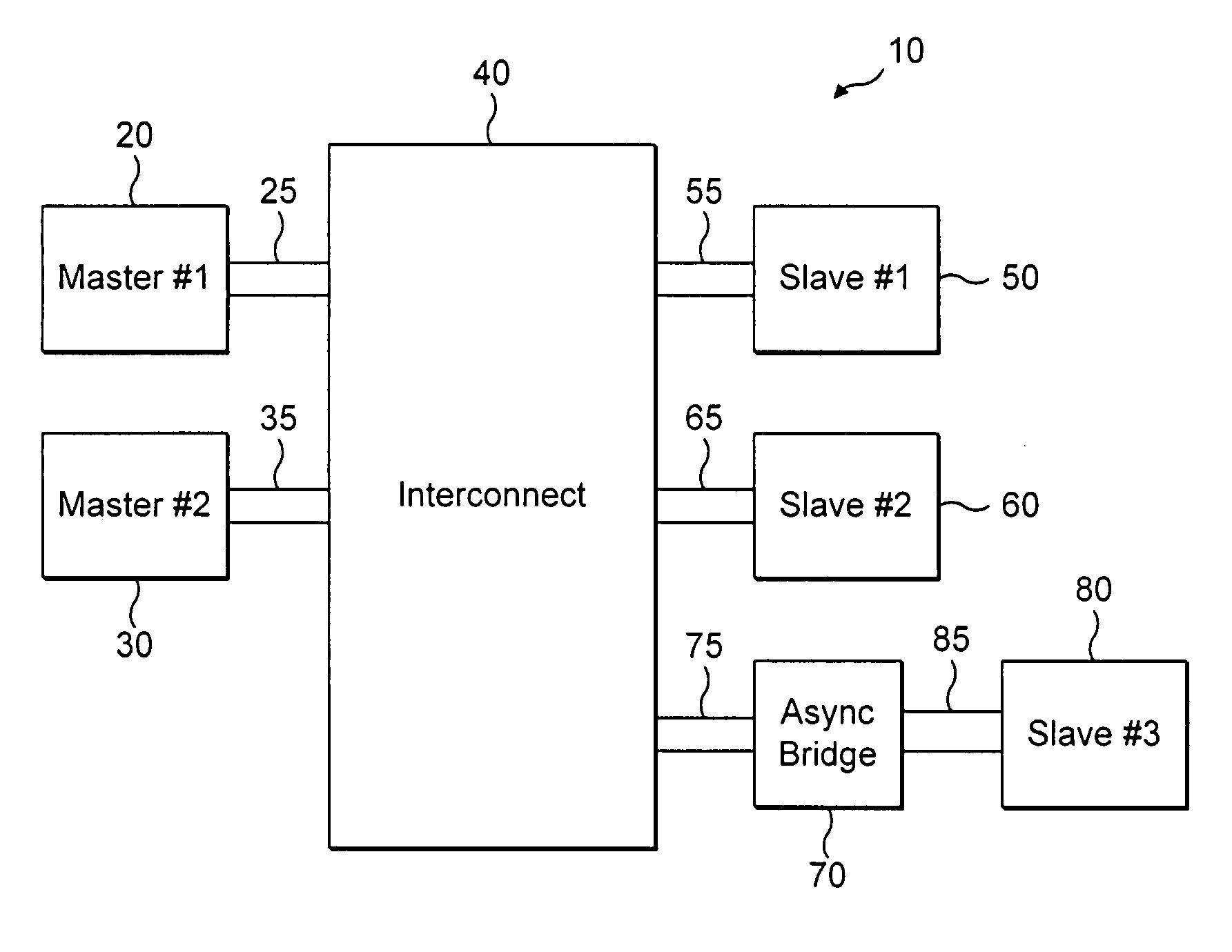
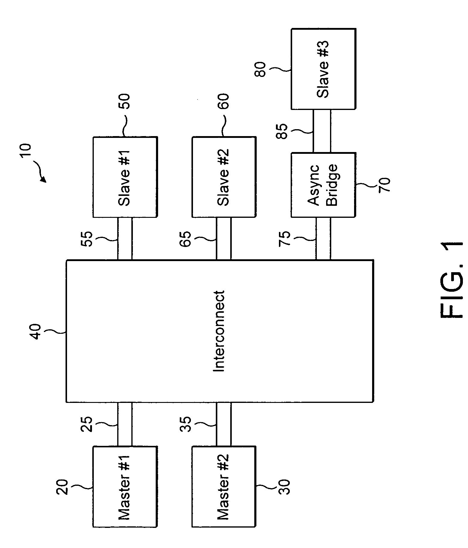
[0025]FIG. 1 illustrates a data processing apparatus in the form of a System-on-Chip (SoC), which may be used within a device such as a personal organiser, a mobile phone, a television set-top box, etc. The SoC design 10 has a plurality of logic elements 20, 30, 50, 60, 70, 80 that are interconnected by an arrangement of buses. The actual interconnection of these buses is specified within an interconnect block or circuit 40. The interconnect block 40 includes a matrix of connection paths which provide for the interconnection of multiple bus master devices and bus slave devices within the SoC 10. Hence, each master device 20, 30 may be connected to corresponding buses 25, 35, respectively, whilst each slave device 50, 60, 80 may also be connected to corresponding buses 55, 65, 85, respectively, with the interconnect block 40 defining how these various buses are interconnected.

[0026] In the example illustrated in FIG. 1, it is assumed that the slave device 80 is provided within a dif...


PUM


Abstract

A data processing apparatus and method of handling write transactions in such an apparatus is provided. The apparatus has a plurality of devices, and bus circuitry providing connection paths between the plurality of devices. At least one of the devices has a bus master interface operable to generate write transactions for output via the bus circuitry, whilst at least one of the devices has a bus slave interface operable to receive the write transactions from the bus circuitry. A write transaction includes transferring a write address from a bus master interface to a bus slave interface and separately transferring write data from the bus master interface to the bus slave interface. In accordance with embodiments of the present invention, the bus master interface is allowed to generate a write transaction such that the write data is received at the bus slave interface before the associated write address. This leads to a significant decrease in the complexity of the apparatus.

Description

BACKGROUND OF THE INVENTION [0001] 1. Field of the Invention [0002] The present invention relates to a data processing apparatus and method, and in particular to techniques for handling write transactions in a data processing apparatus. [0003] 2. Description of the Prior Art [0004] A data processing apparatus may comprise a plurality of devices interconnected by bus circuitry. Data is transferred between the devices via the bus circuitry. One particular type of transfer that may take place is referred to as a write transaction, which is generated by a bus master, and issued via the bus circuitry to a destination bus slave. When generating a write transaction, the bus master will generate a write address identifying an address in memory at which the data the subject of the write transaction should be written, and will separately generate the write data to be written at that address. The write address will be transferred over the bus circuitry separately to the write data. [0005] The ...

Claims


Application Information

Patent Timeline
Patent Type & Authority Applications(United States)
IPC IPC(8): G06F13/00G06F13/40
CPCG06F13/4059
Inventor MATHEWSON, BRUCE JAMESHARRIS, ANTONY JOHN
Owner ARM LTD
Why Eureka
Try Eureka