Organic light emitting device and method of fabricating the same

a light emitting device and organic technology, applied in the direction of identification means, discharge tubes, luminescnet screens, etc., can solve the problems of deterioration of optical characteristics, high production costs, and high cost, and achieve the effect of improving electrical characteristics and optical characteristics of the devi

Active Publication Date: 2005-12-15
SAMSUNG DISPLAY CO LTD
View PDF8 Cites 20 Cited by
  • Summary
  • Abstract
  • Description
  • Claims
  • Application Information

AI Technical Summary

Benefits of technology

[0020] The present invention, therefore, solves aforementioned problems associated with conventional devices by providing an OLED and a method of fabricating the same capable of improving electrical characteristics and optical characteristics of the device by forming a stacked structure of a lower pixel electrode, a reflective layer pattern using Ag and an upper pixel electrode, as a pixel electrode.

Problems solved by technology

As a result, optical characteristics, such as brightness, are deteriorated.
However, when a thin pixel electrode is formed a short circuit is likely to be generated at a step portion of the via-contact hole.

Method used


Image

  • Organic light emitting device and method of fabricating the same
  • Organic light emitting device and method of fabricating the same
  • Organic light emitting device and method of fabricating the same

Examples


Embodiment Construction

[0028] The present invention will now be described more fully hereinafter with reference to the accompanying drawings, in which embodiments of the invention are shown.

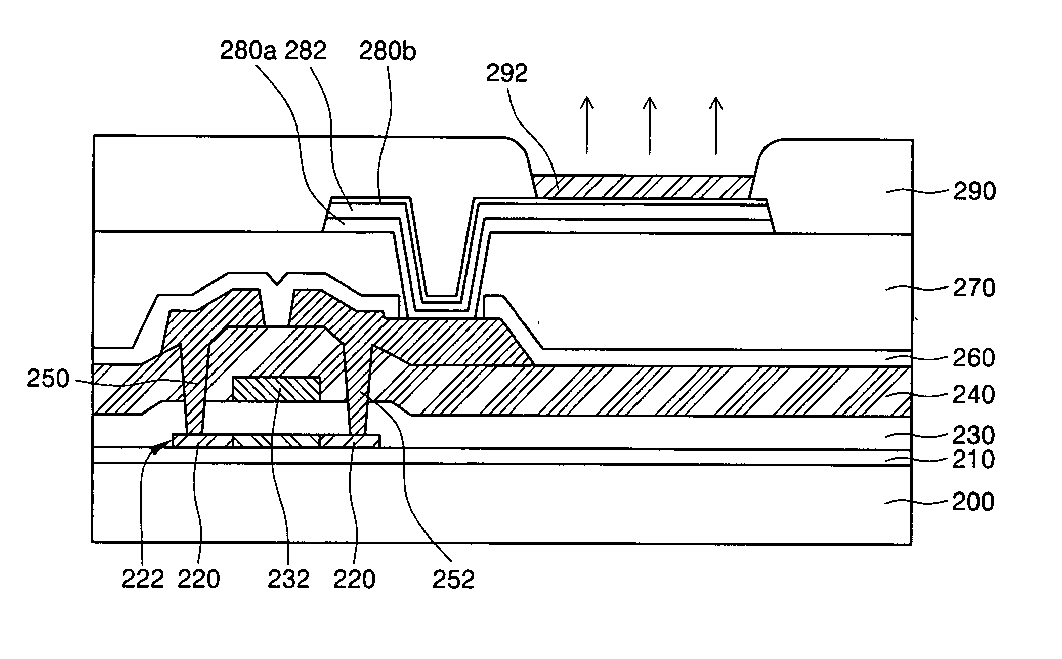
[0029]FIG. 2 is a cross-sectional view of an OLED according to an embodiment of the invention, including a triple-layered pixel electrode having a lower pixel electrode 280a, a reflective layer pattern 282 and an upper pixel electrode 280b on a substrate 200. At the lower pixel electrode 280a is thicker than the thickness of the upper pixel electrode 280b, and the reflective layer pattern 282 may be formed of Ag.

[0030] The organic light emitting display may be formed according to the following operations.

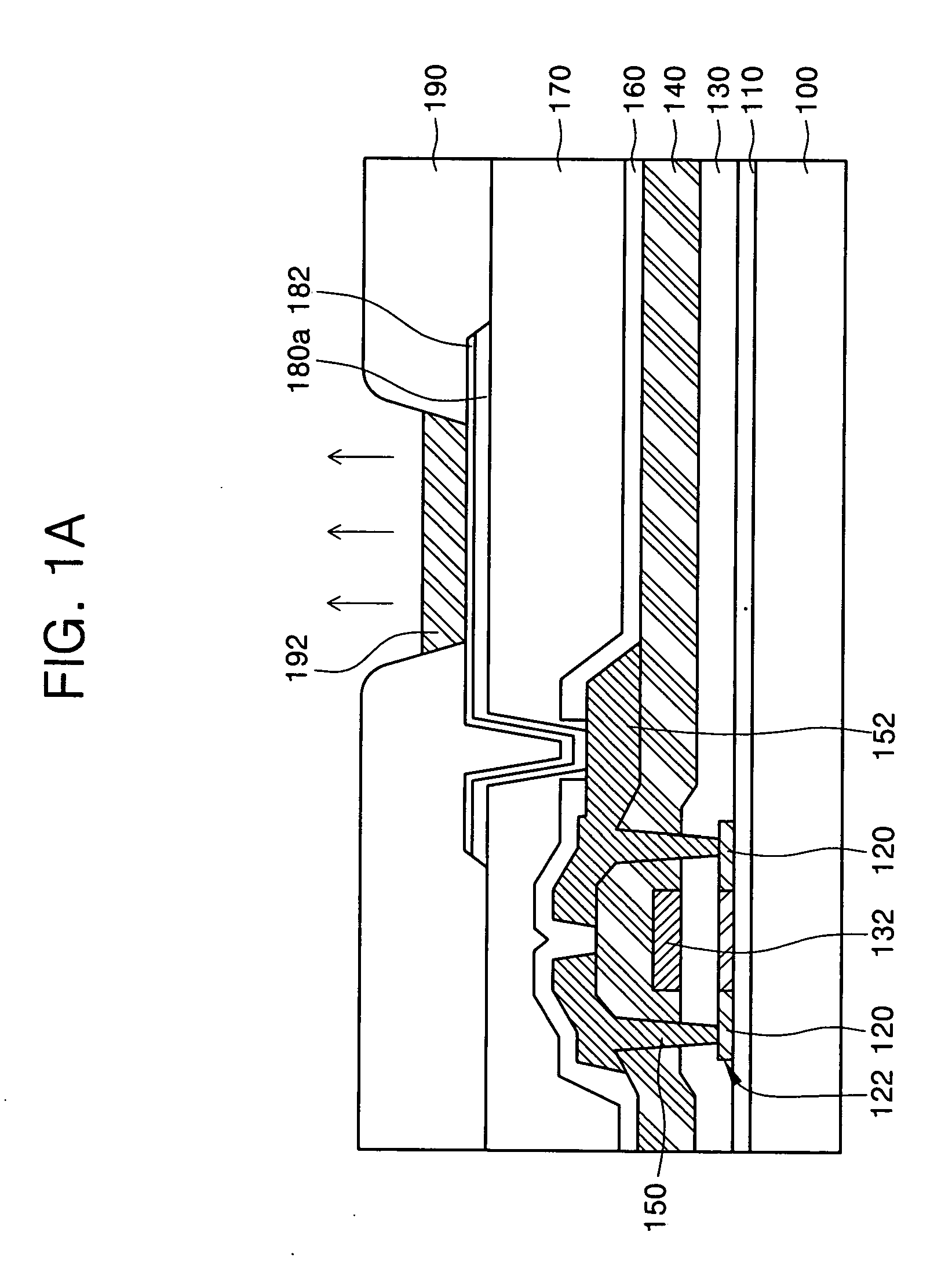
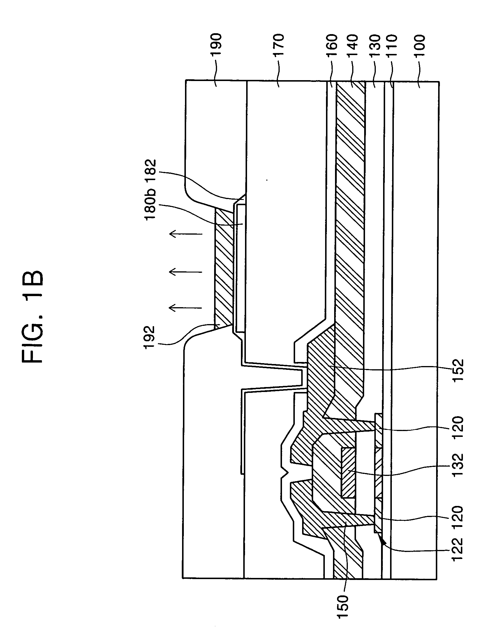
[0031] A buffer layer 210 having a predetermined thickness is formed on an entire surface of a substrate 200 made of glass, quartz, sapphire, or the like. The buffer layer 210 may be formed of silicon oxide using a plasma-enhanced chemical vapor deposition (PECVD) method. The buffer layer 210 prevents impurities in ...


PUM


Abstract

An organic light emitting device (OLED) and a method of fabricating the same are provided, wherein the OLED includes a thin film transistor having a gate electrode, and source and drain electrodes on a substrate; a triple-layered pixel electrode connected to one of the source and drain electrodes through a via-contact hole formed in an insulating layer on the t substrate, and having a lower pixel electrode, a reflective layer pattern and an upper pixel electrode; an organic layer disposed on the upper pixel electrode and having at least an emission layer; and an opposite electrode disposed on the organic layer.

Description

CROSS-REFERENCE TO RELATED APPLICATION [0001] This application claims the benefit of Korean Patent Application No. 2004-38534, filed May 28, 2004, which is hereby incorporated by reference for all purposes as if fully set forth herein. BACKGROUND OF THE INVENTION [0002] 1. Field of the Invention [0003] The present invention relates to an organic light emitting device (OLED) and a method of fabricating the same and, more particularly, to an OLED and a method of fabricating the same, which includes a pixel electrode with a triple-layered structure, having a reflective layer made of Ag interposed, therein. [0004] 2. Description of the Related Art [0005] In general, an OLED is an emissive display device electrically exciting a fluorescent organic compound to emit light. The OLED is classified into a passive matrix OLED and an active matrix OLED depending on the type of driving N×M pixels. The active matrix OLED (AMOLED) is used with large screen displays and has high resolution. Further...

Claims


Application Information

Patent Timeline
Patent Type & Authority Applications(United States)
IPC IPC(8): G09F9/30H01L27/32H01L51/50H05B33/26H01L51/52H05B33/10
CPCH01L27/3244H01L27/3246H01L51/5218H01L51/5271H01L2251/5315H01L2251/558H10K59/122H10K59/12H10K50/818H10K50/856H10K2102/3026H10K2102/351H05B33/26
Inventor SEO, CHANG-SUPARK, MOON-HEEKANG, TAE-WOOKSHIN, HYUN-EOKBAE, SUNG-SIK
Owner SAMSUNG DISPLAY CO LTD
Why Eureka
Try Eureka