

PCB-based surface mount LED device with silicone-based encapsulation structure
- Summary
- Abstract
- Description
- Claims
- Application Information
AI Technical Summary
Benefits of technology
Problems solved by technology
Method used
Image

Examples
Embodiment Construction
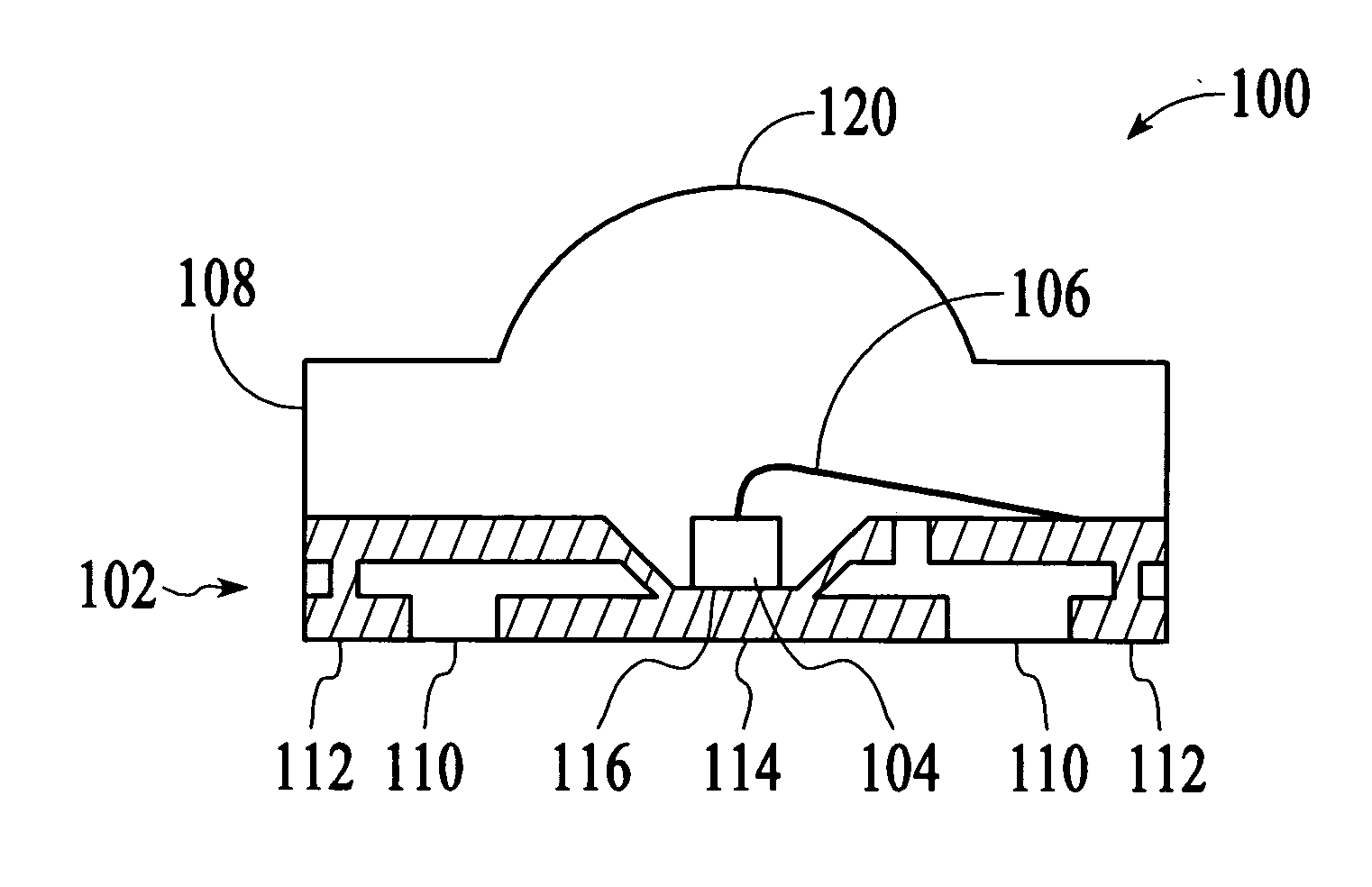
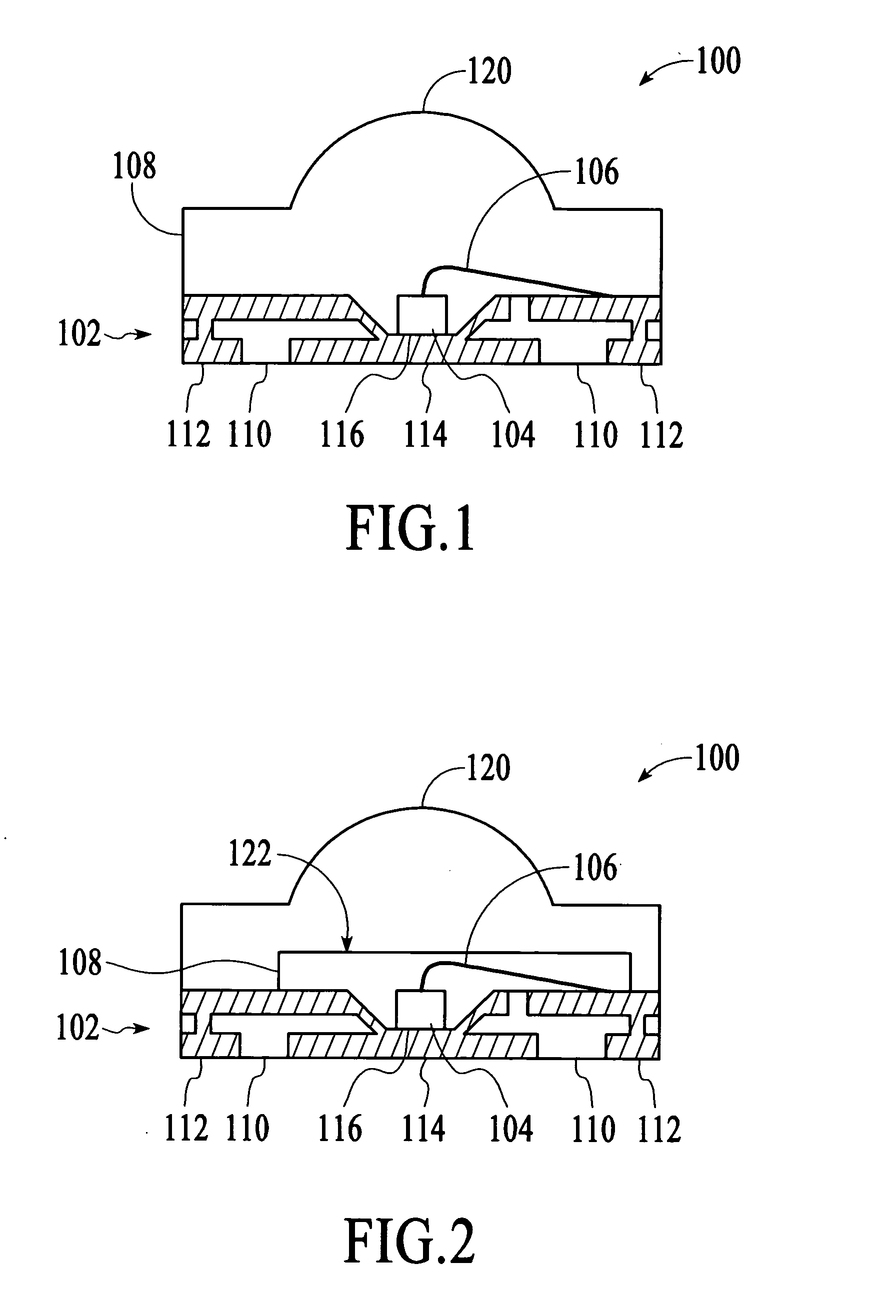
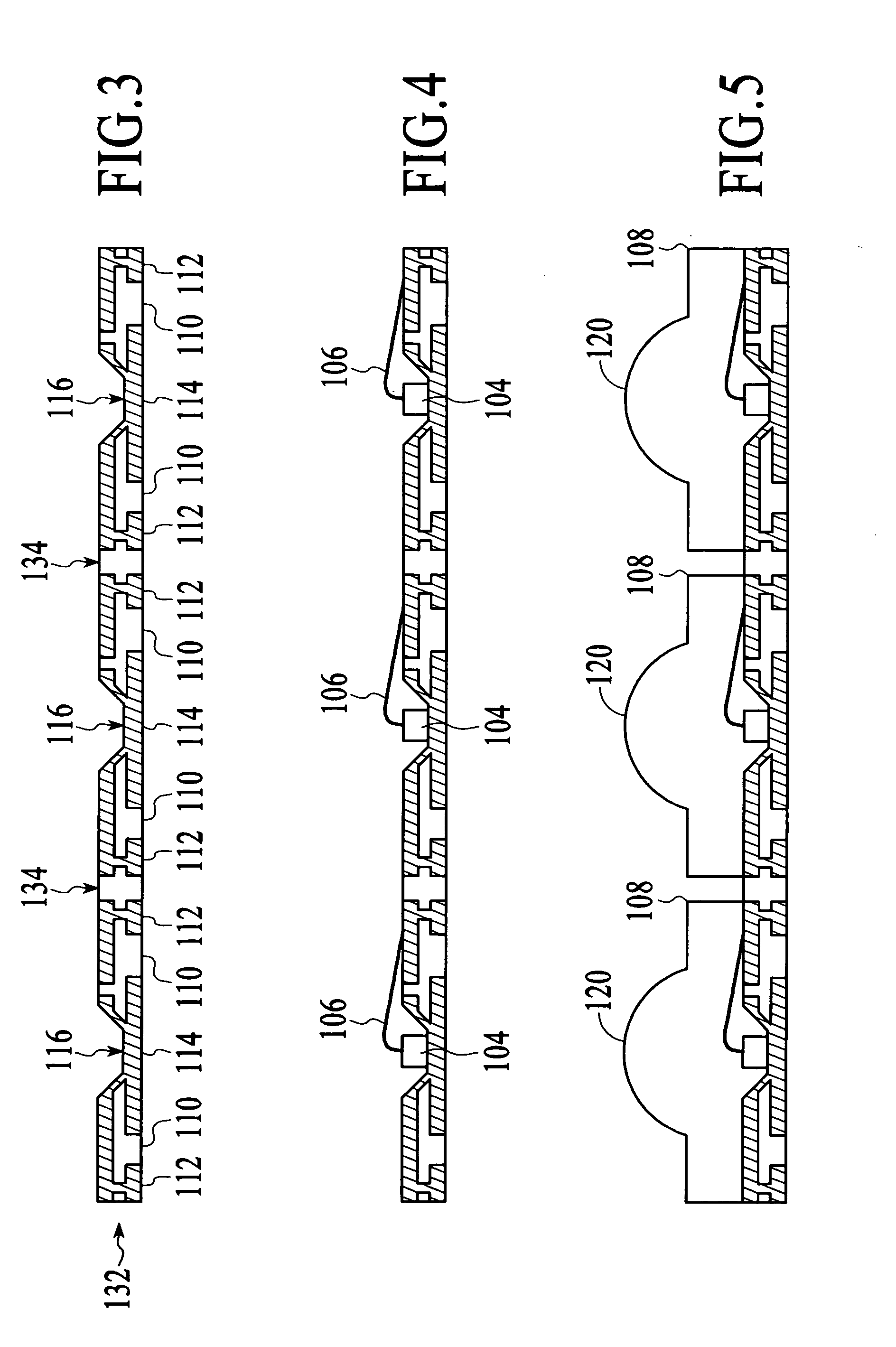
[0014] A light emitting device according to the invention includes a PCB substrate, an LED die that is attached to the PCB substrate, and a silicone-based encapsulation structure that encapsulates the LED die between the silicone-based encapsulation structure and the PCB substrate. FIG. 1 depicts a printed circuit board (PCB) based surface mount light emitting diode (LED) device 100 according to the invention. The PCB-based surface mount LED device includes a PCB substrate 102, an LED die 104, a conductive wire 106, and a silicone-based encapsulation structure 108.
[0015] The PCB substrate 102 includes insulating material 110 and conductors 112 (referred to herein as “leads”). The insulating material electrically separates two leads that enable current to flow through the LED die 104 as is well known in the field. Exposed portions of the two leads are formed to be compatible with surface mount technology and are referred to herein as surface mount-compatible leads. A portion 114 of ...
PUM
 Abstract
Description
Claims
Application Information