High-speed and low-power differential non-volatile content addressable memory cell and array

a non-volatile content, memory cell technology, applied in static storage, digital storage, instruments, etc., can solve the problems of increasing power consumption problems, imposing limitations on array architecture, and further power requirements

Active Publication Date: 2006-01-19
SILICON STORAGE TECHNOLOGY
View PDF13 Cites 35 Cited by
  • Summary
  • Abstract
  • Description
  • Claims
  • Application Information

AI Technical Summary

Benefits of technology

[0008] In the present invention, a differential non-volatile content addressable memory cell comprises a pair of non-volatile storage elements. Each of the non-volatile storage elements has a first terminal, a second terminal and a control terminal for controlling the flow of current between the first terminal and the second terminal. Each of the storage elements is characterized by capable of being in one of two non-volatile states: a first state in which a first current flows between the first terminal and the second terminal and a second state in which a sec

Problems solved by technology

Although the content addressable memory array 10 is of high speed because the memory cell 12 uses an SRAM as the storage element, it is volatile and further has high power requirements.
Since t

Method used


Image

  • High-speed and low-power differential non-volatile content addressable memory cell and array
  • High-speed and low-power differential non-volatile content addressable memory cell and array
  • High-speed and low-power differential non-volatile content addressable memory cell and array

Examples


first embodiment

[0018] Referring to FIG. 4, there is shown a differential non-volatile content addressable memory cell 40 of the present invention. The cell 40 comprises a pair of non-volatile storage elements 42a and 42b. Each non-volatile storage element 42 has three terminals: a first terminal labeled “A,” a second terminal labeled “B,” and a third terminal labeled “C.” Each of the storage elements 42 is capable of being in one of two non-volatile states: a first state in which a first current flows between the first terminal A and the third terminal C and a second state in which a second current, less than the first current, flows between the first terminal A and the third terminal C. The second terminal B is a control terminal that controls the flow of current between the first terminal A and the third terminal C. The cell 40 also comprises a pair of differential data lines 18 labeled as “compare 18a” and “compare bar 18b.” Each of the data lines 18 is connected to the second terminal B of one...

second embodiment

[0030] Referring to FIG. 5, there is shown an improved differential non-volatile content addressable memory cell 50. The memory cell 50 comprises a pair of non-volatile storage elements 42a and 42b, each of which can be of the embodiment shown in FIGS. 6A-6J. As previously discussed, each of the non-volatile storage elements 42 comprises three terminals: a first terminal A, a third terminal C, with a second terminal B controlling the conduction of current between terminal A and terminal C. The first terminal A of the two storage elements 42a and 42b are connected to the match line 14. The match line 14 is connected through a load 45 to Vcc. The terminals B of each of the storage elements 42a and 42b are connected to the compare line 18a and compare bar lines 18b, respectively. Finally, the terminal C of the two storage elements 42a and 42b are connected together and in common to a control line T3. During operation, the voltage supply on the control line T3 is at a second voltage whi...

third embodiment

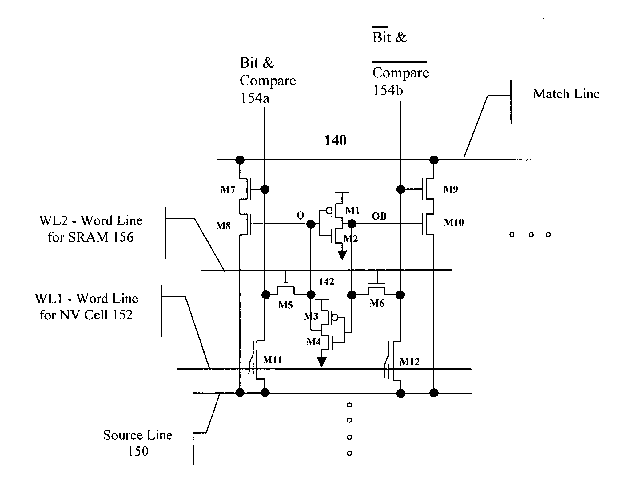
[0032] Referring to FIG. 8 there is shown a circuit diagram of a memory cell 140 of the present invention. The memory cell 140 shown in FIG. 8 comprises a volatile memory cell 142, for storing Q and Q(Bar) of the data. The transistors M1, M2, M3 and M4 form the volatile memory cell 142. The cell 140 also comprises two non-volatile single transistor cells M11 and M12, for storing Q and Q(Bar) of the data respectively. Although single transistor memory cell of the type shown in FIG. 6C (or 6D) is shown as being used for the memory cell M11 or M12, other types of non-volatile memory transistors may also be used. A source line 150 connects to the first (source or drain) region of the transistors M11 and M12. A first word line 152 connects to the gates of the transistors M11 and M12. A bit / compare line 154a connects to the second (drain or source) region of the transistor M11; a bit(bar) / compare(bar) line 154b connects to the second (drain or source) region of the transistor M12. Transis...


PUM


Abstract

A differential non-volatile content addressable memory array has a differential non-volatile content addressable memory cell which uses a pair of non-volatile storage elements. Each of the non-volatile storage elements can be a split-gate floating gate transistor or a stack gate floating gate transistor having a first terminal, a second terminal, a channel therebetween and a floating gate over at least a portion of the channel to control the conduction of electrons in the channel, and a control gate. The floating gate storage transistor can be in one of two states: a first state, such as erase, in which current can flow between the first terminal and the second terminal, and a second state, such as programmed, in which substantially no current flows between the first terminal and the second terminal. A pair of differential compare data lines connects to the control gate of each of the pair of non-volatile floating gate transistors. A match line connects to the first terminal of each of the pair of non-volatile floating gate transistors to a first voltage. Finally, the second terminals of each storage element is connected to a second voltage, different from the first voltage. A current passing through the memory cell is indicative of a mis-match between the contents of the compare data lines and the contents of the storage elements.

Description

TECHNICAL FIELD [0001] The present invention relates to a differential non-volatile content addressable memory cell and array that is capable of high-speed and low-power operation. More particularly, the present invention relates to a high-speed, low-power differential non-volatile content addressable memory cell either binary or ternary and an array using a compare data line that is isolated from the conducting channel. BACKGROUND OF THE INVENTION [0002] Content addressable memory cell and array are well known in the art. See, for example, U.S. Pat. Nos. 6,078,513; 5,949,696; 5,930,161; and 5,051,943. A differential non-volatile content addressable memory cell and array is also well known in the art. See, for example, U.S. Pat. No. 6,005,790. [0003] Referring to FIG. 1, there is shown a binary differential volatile content addressable memory array 10 of the prior art. In this memory array 10, a differential content addressable memory cell, such as cell 12a, is comprised of pair of ...

Claims


Application Information

Patent Timeline
IPC IPC(8): G11C15/00
CPCG11C15/046G11C14/00
Inventor SARIN, VISHALTRAN, HIEU VANNOJIMA, ISAO
Owner SILICON STORAGE TECHNOLOGY
Why Eureka
Try Eureka